


Contents

On-demand webinar
How Good is My Shield? An Introduction to Transfer Impedance and Shielding Effectiveness
by Karen Burnham
Signal Integrity (SI) signifies the signal’s ability to propagate along PCB traces without distortion. Signal integrity is about the quality of the signal passing through a transmission line. In this article, Tim Wang Lee acknowledges some of the designers’ pain points regarding robust PCB design workflow and signal integrity.
About the presenter:
Tim Wang Lee, signal integrity application scientist, Keysight Technologies.
Q1: How to achieve a robust PCB design?
Tim Wang Lee: To achieve a robust PCB design workflow consider the following points:
- Understand possible root causes of signal integrity issues.
- Create a virtual prototype using Electronic Design Automation (EDA) software.
- Rely on a dependable manufacturer for layout, fabrication, and assembly and that will be Sierra Circuits.
Q2: What is the difference between traditional design and the robust design approach?
Tim: In a traditional design, we fabricate the prototype once we create a design and layout based on our vendor guidance. In the case of a robust electronic circuit design approach, we create a virtual prototype, simulate and validate the prototype after creating the design.
Transient analysis is one of the key aspects to ensure signal integrity in your design. To learn more about it, see Transient Analysis for Non-Sinusoidal Signals.
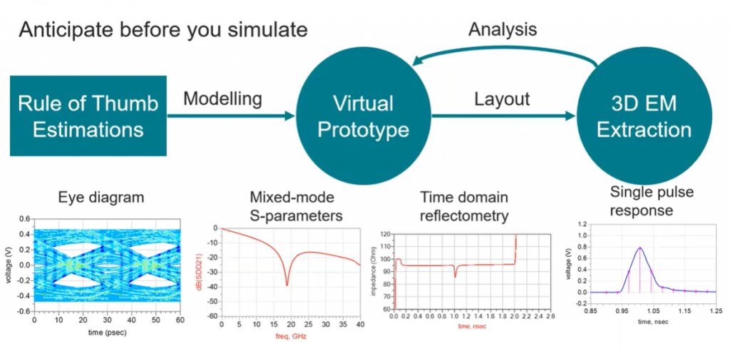
Q3: What are the advantages of having a virtual prototype?
Tim: A virtual prototype helps us to troubleshoot and understand the design in an efficient manner. Investing a little more time in creating a virtual prototype gives you a lot in return. It also helps us to achieve better signal integrity. The advantages are summarized in the below image.

The effort is a little higher, but the ability to troubleshoot and perform what-if-analysis increases.

Signal Integrity eBook
6 Chapters - 53 Pages - 60 Minute ReadWhat's Inside:
- Impedance discontinuities
- Crosstalk
- Reflections, ringing, overshoot and undershoot
- Via stubs
Download Now
Q4: What is the robust design workflow for signal integrity?
Tim: The signal integrity workflow is as follows:
- Rule of thumb estimations – this addresses signal integrity issues
- Create a virtual prototype
- 3D extraction
- Perform what-if-analysis
The workflow diagram is shown below:

To know more about signal integrity analysis, read our article Unlock Your Signal Integrity Analysis Potential.
Q5: What are the rules of thumb to be followed?
Tim: The rules of thumbs are as follows:
- 8-7-3 rule:
- 8dB loss at Nyquist, Eye with 75% UI jitter, 30% height
- 0.1-0.2 dB/inch/GHz:
- 0.1-0.2 dB of loss per inch per GHz for transmission line
- Single-ended 50 ohms (FR4)
- Microstrip impedance: Width/Height = 2 – width of the trace is twice the substrate height.
- Stripline impedance: Width/Height = 1 – width of the trace is the same as min of the substrate heights.
- Differential 100 ohms (FR4):
-
- Spacing = 3W uncoupled; Differential impedance = 2 times single-ended impedance.
- Move the traces closer, this decreases differential impedance.
- Stub resonance (GHz) for FR4 is 1.5/stub length (inches)
Q6: What is the minimum trace width?
Tim: The typical specification for the minimum trace width is 6 mils. There are also premium options that give you a trace width lower than 6 mils.

Q7: I don’t have any signal integrity background, how can I learn it?
Tim: Sierra Circuits offers you a lot of educational content.
You can check out understanding signal integrity article to learn more about signal integrity.
You can also refer to the following resources:
- ADS Signal Integrity Workshop
- PathWave ADS Free Trial
- Videos on simulation and measurement
- How to Solve Signal Integrity Problems: The Basics
Q8: Are there any particular edge classes for which this design framework doesn’t work?
Tim: I will say this design framework will work well especially for corner cases because it is designed not to confine ourselves, but give ourselves flexibilities. Take controlled impedance line designer (shown below) for example, once you know the stack-up, you can vary the substrate material properties or even the conductor roughness. It’s giving you more freedom to explore these edge cases.

Q9: Is there any advantage or preference for running differential pairs on inner layers versus on top layers for signal integrity or externally injected or radiative EMI reasons?
Tim: Yes, for sure. That’s why we use differential traces. If you assume the same kind of noise on the positive trace and the negative trace, when you take the difference, the common noises will cancel each other out because they are common to both.
Q10: Can these techniques be applied to lower-speed circuits?
Tim: You can always apply these techniques to design at a lower speed. As we’ve seen in the cases when we are scaling up the data rate, the longest allowed transmission line becomes shorter. If the data rate goes lower, that means you can tolerate a longer line, which means a lower data rate is a bit easier to design, just because the loss is a lower data rate. You can apply all these techniques to lower data rates.
Q11: How are the rules of thumbs affected by going to higher speed material?
Tim: With most of the rules of thumb here (shown below), if there’s a requirement for data rate, say for the loss, the rule of thumb will have a frequency term, dB per inch per GHz. As long as you scale your data rate to your Nyquist frequency, all these will work the same for higher data rate, higher speed material, with the caveat that the material property has to be close enough to FR4. If you’re using say silicon, it’s going to be different, but you can always rely on your simulator in that case.

Q12: Can we get an evaluation license for free?
Tim: You can always get an evaluation license for free. Check PathWave Advanced Design System (ADS) Software to know more about it. As far as pricing goes, we have different bundles that would make it easier for you to perform what you need to do at an affordable price.
Q13: Is there a direct way to move the transmission line multi-layer library stack-up to the control impedance tool?
Tim: Yes, the control impedance line tool requires you to have the stack-up.
Q14: Can process variation be included in the simulation?
Tim: Yes, process variation can be included in the simulation.
A good PCB layout and design is a complex task with many challenges. Special attention must be paid to ensure the line impedances are carefully matched and the discontinuities are avoided. It is essential to by heart the basics of transmission line theory and to understand the transmission line effects in high-speed PCB design.

High-Speed PCB Design Guide
8 Chapters - 115 Pages - 150 Minute ReadWhat's Inside:
- Explanations of signal integrity issues
- Understanding transmission lines and controlled impedance
- Selection process of high-speed PCB materials
- High-speed layout guidelines
Download Now
About Milan Yogendrappa : Milan Y is an electronics and communication engineer with over 6 years of experience in developing and editing technical articles related to PCB design, manufacturing, and assembly. He is currently the editor-in-chief at Sierra Circuits.


