


Contents
Ensuring a smooth assembly process requires meticulous planning during the design phase. To achieve this, it is critical to know common design mistakes that result in PCB assembly errors.
Incomplete design data, improper component placement, insufficient clearances, and poor thermal management lead to board assembly errors such as overlapping components, pad lifting, and solder bridges.
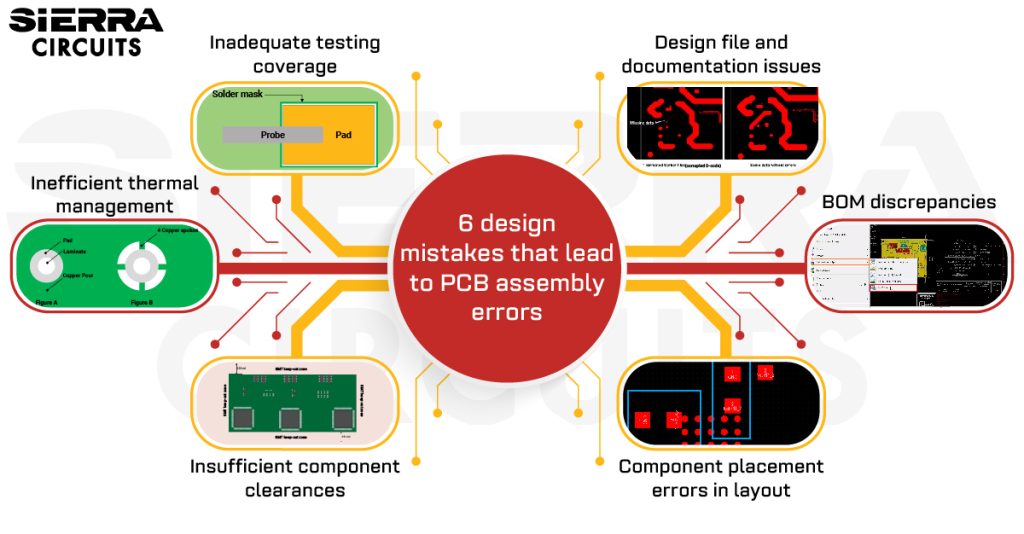
In this article, you will learn the 6 common design mistakes that result in PCB assembly defects. By understanding and avoiding these design pitfalls, you can ensure an error-free assembly process, reduced PCBA costs, and improved product quality.
6 common design mistakes that cause PCB assembly errors
1. Design file and documentation mistakes
PCBA requires detailed documentation to communicate the design intent to your manufacturers. Discrepancies in the design data can lead to various assembly defects, such as incorrect footprints, silkscreen, and solder mask errors. Here are some prevalent Gerber, centroid, and solder paste stencil file errors to watch out for to ensure an effective circuit board assembly process.
1.1 Gerber file defects
- Missing or misaligned layers: Any layers, such as signal, ground, power, and solder mask layers, are overlooked from the Gerber files.
- Incorrect layer order: The layer sequence in the Gerber files does not match the intended stack-up.
- Drill hole errors: Errors in drill hole counts, positions, and sizes can lead to part misalignment during PCB drilling.

- File format errors: Incorrect file formats, outdated standards, and corrupted files can lead to miscommunication between you and your CM.

Ways to avoid Gerber file errors:
- Make sure the design units and precision settings are consistent across all design files.
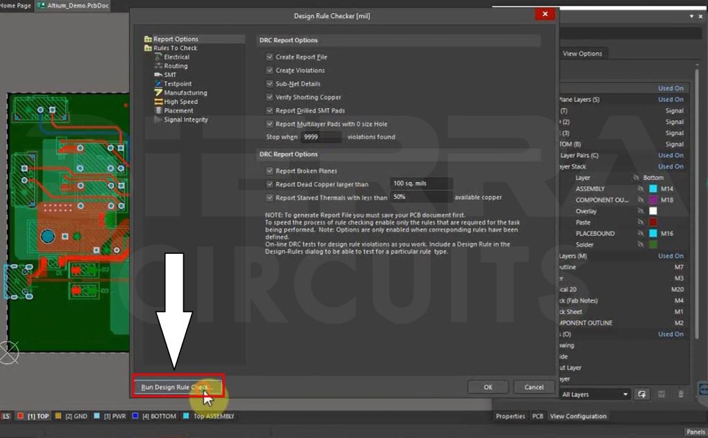
- Thoroughly review your design before generating Gerber files. In addition to that, run a DRC to identify any PCB layout or component placement errors. For more, read common problems associated with Gerber files.
1.2 Centroid file errors
- Incorrect coordinates: Mismatched component coordinates can lead to the assembly of components in the wrong locations.
- Incorrect orientation: Wrong orientation of reference designator and components.
Ways to avoid centroid file issues:
- Ensure the component positions in the centroid file match the actual positions on the layout.
- Verify the coordinate units in the centroid file match the units used in the assembly process (e.g., millimeters or inches).

1.3 Solder paste stencil file issues
The stencil file configures the stencil for the solder paste application right before component placement.
- Incorrect aperture sizes: Incorrectly sized openings in the stencil can lead to insufficient or excessive solder paste, affecting soldering quality.
- Misaligned apertures: If the apertures in the SMD stencil file are misaligned with the pad positions, solder paste can be misapplied.
- Aperture overlaps: Apertures overlapping with the neighboring pads and components can cause short circuits.

How to avoid solder paste stencil errors
- Choose an appropriate stencil thickness based on component sizes, pad designs, and solder paste requirements. Use the following formula to select the proper stencil thickness:
-
- Stencil thickness = Aperture width/stencil aspect ratio

2. Apply fiducial marks to both the panel and the stencil for accurate stencil alignment. The diameter of fiducial marks should be between 1 and 3 mm.
3. Maintain at least 3 mm clearance between the board edge and the fiducials.
4. For best accuracy, place 3 global fiducials on the edges, and position at least 2 local fiducials diagonally to the SMT component.

1.4 Inaccurate assembly drawings
- Ambiguous instructions: Unclear instructions in the assembly drawing can lead to misunderstandings during the assembly process.
- Mismatched component designators: Mismatches between the designator labels on the assembly drawing and the actual board can result in incorrect component placements.
- Missing polarity markings: Missing polarity markings and silkscreen indicators can lead to improper orientation of polarized components such as diodes and capacitors.
Ensure your assembly drawings include correct data on component references, part numbers, values, and special instructions. To learn more, read PCB assembly notes.

1.5 Inefficient CAD file conversion
Inefficient CAD file conversion may lead to:
- File format incompatibility: Using incompatible file formats for conversion can result in data loss, missing layers, and incorrect dimensions.
- Incorrect unit settings: Incorrect unit settings during the conversion can cause misalignments and improper component placements.
- Geometry distortions: Conversions might introduce geometrical distortions, such as rounded corners becoming jagged.
- Pad and via shape errors: If the conversion doesn’t accurately translate pad and via shapes, it can result in incorrect solder pad sizes, nonfunctional vias, and unreliable connections.
To trim down these errors, make sure the file format is supported by both the CAD and CAM software.

PCB Design for Assembly Handbook
6 Chapters - 50 Pages - 70 Minute ReadWhat's Inside:
- Recommended layout for components
- Common PCB assembly defects
- Factors that impact the cost of the PCB assembly, including:
- Component packages
- Board assembly volumes
Download Now
2. BOM discrepancies
2.1 Incorrect part numbers
Using the wrong part numbers or providing incorrect descriptions for components can result in the wrong components being sourced.
2.2 Missing components
Missing components in the BOM can result in incomplete assemblies.
2.3 Duplicate entries
Listing the same component multiple times can lead to confusion during component sourcing and stocking. Also, this can cause over-ordering of components.
2.4 Incorrect quantities
Providing incorrect quantities for components can lead to shortages or excess inventory.

2.5 Obsolete parts
Including components that are obsolete or no longer available for purchase can lead to delays in production.
2.6 Incorrect vendor information
Providing incorrect vendor names, part numbers, and lead times can delay the procurement process.
How to ensure a clean BOM
- Verify BOM information with component datasheets to validate accuracy. Try the BOM Compare Tool to compare two BOM files.
- Validate BOM entries with the reference designators in the design files to ensure consistency and prevent duplication.
- Double-check vendor details, part numbers, and lead times to manage the assembly errors.
- Estimate component quantities accurately as per the assembly requirements.
- Regularly review and update the BOM to identify obsolete components and restock them with suitable alternatives.
- Implement a checklist to cross-check the BOM against the design files.
To avoid risks associated with component procurement and storage, consider leveraging our COIN services—a comprehensive PCB component sourcing and stocking program tailored to prevent part obsolescence, supply shortages, extended lead times, and all BOM-related issues.

3. Component placement errors in the Gerber file
3.1 Incorrect orientation
Placing components in the wrong orientation can lead to reversed polarity, improper connections, and incorrect functionality.
- To avoid inaccurate orientation, review datasheets and documentation of polarized components such as diodes and electrolytic capacitors. Mark their pin 1 position correctly in the footprints.

3.2 Misaligned components

Misaligned components can result in soldering issues and tombstoning.
To avoid component misalignment:
- Include clear component outlines and reference centroids.
- Maintain a 1:1 ratio between solder mask openings and pads.
3.3 Incompatible component height sequence during wave soldering
The sequence of the component height is often overlooked during the wave soldering process. If smaller components are shadowed by the larger components, the quality of the soldering will be hampered.

To avoid this, place the taller components behind the shorter ones, as shown in the image.
3.4 Incorrect footprints
If a component footprint doesn’t match the component’s physical dimensions, it can lead to assembly errors.

You need to validate component datasheets to ensure accurate footprint creation.
4. Insufficient component clearances
4.1 Inadequate component-to-component clearance
To avoid assembly errors that result from insufficient component clearance, stick to the following guidelines:
- Components smaller than 0603 packages should have 6 mil clearance
- Sensitive devices like BGA should have a clearance of 39 mil
- Connectors, crystals, and canned capacitors need a minimum of 20 mil clearance
- Have at least 10 mil of courtyard clearance for all the components

- Here are the spacing requirements between two passive components when they are mounted side-by-side:
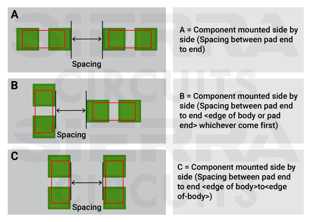
| Component type | 0201 | 0402 | 0603 | 0805 | 1206 | ||||||||||
|---|---|---|---|---|---|---|---|---|---|---|---|---|---|---|---|
| Mounting style | A | B | C | A | B | C | A | B | C | A | B | C | A | B | C |
| 0201 | 12 | 15 | 10 | ||||||||||||
| 0402 | 12 | 15 | 10 | 12 | 18 | 10 | |||||||||
| 0603 | 12 | 18 | 10 | 15 | 20 | 10 | 15 | 20 | 12 | ||||||
| 0805 | 15 | 20 | 12 | 18 | 20 | 15 | 18 | 25 | 15 | 20 | 30 | 18 | |||
| 1206 | 15 | 20 | 12 | 18 | 25 | 15 | 20 | 25 | 18 | 25 | 30 | 20 | 25 | 30 | 20 |
4.2 Component-to-copper feature clearance violations
Components placed close to the traces can result in shorts due to solder wicking.
Follow these standards to ensure sufficient clearance between components and copper features:
- Incorporate at least 8 mil part-to-hole distance
- The spacing between the component pad and the annular ring edge should be a minimum of 7 mil

4.3 Component-to-board edge clearance
Components placed on the board edge can be more susceptible to damage during handling, and they might not be properly soldered during the reflow process.
To provide adequate clearance for cutting tools and prevent any potential damage:
- Position the components 50 to 75 mil away from the board edge.
- For taller components like electrolytic capacitors, maintain a clearance of 125 mil from the board edge.
- Incorporate a 20 to 25 mil spacing between the board edge and SMD components to avoid physical damage during depanelization.
- Spacing for copper traces and manually installed parts (mixed assembly technology) should be 10 mil for outer layers and 15 mil for inner layers.

As a designer, you need to ensure optimum clearance between components and traces to optimize your designs for testing.
4.4 Insufficient solder mask to pad clearance
Insufficient solder mask clearances can lead to various PCB assembly errors, such as solder mask encroachment and poor solder connections. Also, this reduces the component life cycle and overall reliability of your board.

To address this issue, incorporate a solder mask dam of around 1.6 mil between two pad edges to avoid solder mask encroachment.
5. Inefficient thermal management
5.1 Inadequate heat dissipation
Inadequate heat dissipation increases the operating temperatures of the components over their temperature ratings.
To avoid this:
- Incorporate proper cooling mechanisms such as heatsinks, thermal vias, and fans to dissipate heat from components
- Identify the hotspots and optimize the component placement to allow for efficient heat dissipation

To learn how to optimize thermal management in your design, read PCB heat dissipation techniques by Keven Coates.
5.2 Insufficient thermal relief for through-hole components
Insufficient thermal relief connections for through-hole components can hinder the proper transfer of heat to the copper plane and lead to poor soldering joint reliability.
- Design footprints with adequate thermal relief connections to ensure proper heat transfer during soldering
- Use a minimum of 4 spokes evenly distributed around the pad for balanced heat dissipation
- The spoke width should be one-third to one-half of the pad diameter
- Maintain a uniform spacing between the spokes for consistent thermal relief distribution

5.3 Blocked airflow paths
Blocked paths can trap heat and cause components to exceed their temperature limits. It occurs due to dense component placement, misaligned solder mask with the thermal vias, and if parts are placed directly over heatsinks.
Stick to these guidelines to avoid blocked airflow paths:
- Optimize component placement to allow adequate space for airflow around components
- Ensure proper alignment of the solder mask with thermal vias to prevent obstruction of airflow paths

6. Impaired PCB testing coverage
To improve the coverage of the testing procedure, develop a comprehensive test plan that outlines which components, traces, and connections need to be tested.
Preferred test points are:
- Test pads without solder resist
- Vias
- Through-holes
- PTH and SMD component pads

Make sure there is no solder mask on the test point. The solder mask should not be tangent to the test point.
Follow these DFT guidelines to design an efficient test fixture:
- The minimum distance between a test point and the component can be estimated
by the formula:L = (0.29 x height) + 0.7 (in mm)

- Design high-quality test fixtures that ensure proper alignment and contact with test points.
- CAD data must include the component height. The design team provides a list of components whose height is over 17 mm.
For more guidelines on test points, download the Design for Testing Handbook.

Design for Testing Handbook
7 Chapters - 28 Pages - 45 Minute ReadWhat's Inside:
- PCB testing strategies
- Guidelines to design and place a test point for FPT
- Directives to make your board ICT compatible
- Benefits and drawbacks of various testing methods
- Defects that you can identify through board testing
Download Now
A successful PCB assembly process requires attention to detail during the design phase. Comprehensive design data, clean BOM, sufficient clearances between components and copper features, and efficient thermal management ensure a smooth assembly process.
To avert the potential design mistakes that hamper the assembly process, stick to our PCB Design for Assembly Checklist.
Please let us know in the comments section if you require any assistance to optimize your PCB design to streamline the assembly process. Our experts will be happy to help you.
About Poulomi Ghosh : Poulomi is a microwave engineer specializing in EMI, EMC, RF, and high-speed electronics. As a senior technical writer at Sierra Circuits, she creates advanced engineering articles and webinars for hardware engineers and PCB designers.


Start the discussion at sierraconnect.protoexpress.com