Contents
Impedance is the measurement of the restriction imposed by a circuit on the current flow. It is similar to resistance, but it also considers the effects of inductance and capacitance. Impedance control in flex stack-ups is essential to reduce signal reflections and achieve signal integrity.
Controlled impedance (CI) is the characteristic impedance of a transmission line in a PCB conductor and its related reference planes. It is especially required when high-frequency signals propagate through a circuit board trace.
Why do you need controlled impedance for flex PCBs?
In modern days, flex circuit boards have become smaller, faster, and more complicated. Flex boards are typically used in high-frequency applications such as RF communication, telecommunication, computing using signal frequencies above 100MHz, high-speed signal processing, and high-quality analog video such as DDR, HDMI, Gigabit Ethernet, etc.
Signal traces have impedance at each point on the signal path. If this impedance varies from point to point, a signal reflection will occur whose magnitude depends on the difference between the two impedances. This reflection will travel in the opposite direction of the signal, which means the reflected signal will superimpose the original signal.
For a better understanding of controlled impedance, read why controlled impedance really matters.
What is impedance matching in PCBs?
Impedance matching becomes essential for flex PCB design as they are generally used in high-speed applications. It refers to matching the load impedance to the transmission line’s characteristic impedance. If the load impedance and the characteristic impedance are equal, the reflections in the circuit board transmission line will be eliminated. This ensures that the original data is received without signal attenuation.
Factors affecting impedance in flex circuit board stack-up
Impedance control in flex can be achieved by altering the PCB traces’ physical dimensions and the dielectric material’s properties. Below are the factors that affect impedance in flex PCBs.
Physical dimensions of the traces
- Height of the trace
- Width of the top surface of the trace
- Width of the bottom surface of the trace
- Difference between the width at the top of the trace and the bottom of the trace
- Height of the trace from the ground plane
Dielectric properties of the dielectric material used
- The dielectric constant of the dielectric material incorporated
- Dielectric height between the trace and the reference plane
- The dielectric constant of the solder mask or coverlay
Stick to these design rules to build a reliable flex PCB stack-up.

Controlled impedance configurations for flex boards
The most common configurations used for impedance control in flex boards are:
Single-ended microstrip
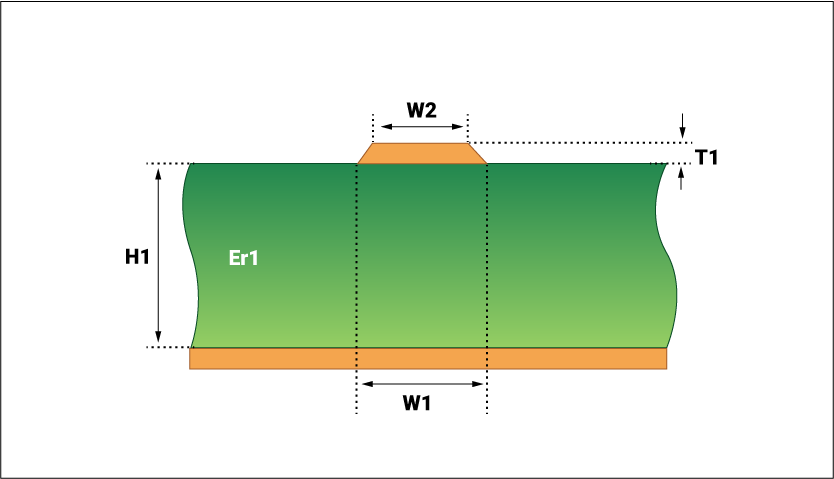
H1: Height of the dielectric between the trace and the reference plane
W1: Width of the bottom surface of the trace
W2: Width of the top surface of the trace
T1: Thickness of the trace
Er1: Dielectric constant of dielectric between the trace and the reference plane
This configuration has a transmission line made of a uniform conductor (thickness and width) on the outer layer of the board stack-up. The reference plane provides the current return path for the signals traveling on the transmission line. Single-ended microstrip allows for thinner flex construction, increasing flexibility and reducing the overall cost.
Edge-coupled coated differential microstrip
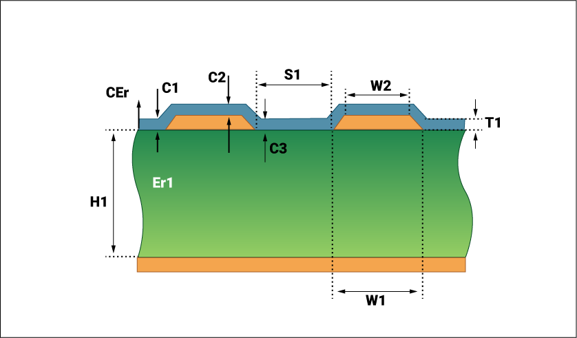
H1: Height of the dielectric between the trace and the reference plane
W1: Width of the bottom surface of the trace
W2: Width of the top surface of the trace
T1: Thickness of the trace
S1: The separation between the two traces of the differential pair
C1, C2, and C3: Thickness of the coverlay at various locations
CEr: Dielectric constant of coverlay
When a signal and its complement are transmitted on two separate traces, it is called differential signaling. These traces are called differential pairs. The traces are routed with a constant space between them. One of the primary advantages of having edge-coupled differential pairs is that the noise on the reference plane is common to both traces, canceling out the noise at the receiver end.
To learn how to design flex boards with differential pairs, see handling differential pairs in flex PCBs.

Single-ended stripline
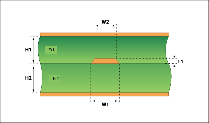
H1: Height of the first dielectric
H2: Height of the second dielectric
W1: Width of the bottom surface of the trace
W2: Width of the top surface of the trace
Er1: Dielectric constant of the first dielectric
Er2: Dielectric constant of the second dielectric
T1: Thickness of the trace
It implements the signal trace between two ground planes in a multi-layer PCB. The return path for a high-frequency signal is located above and below the signal trace on the planes.
Edge-coupled differential stripline
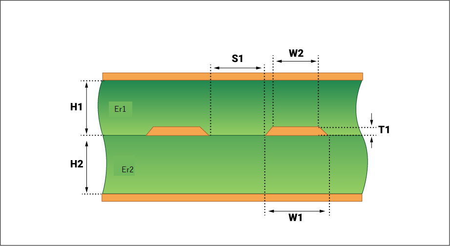
H1: Height of the first dielectric
H2: Height of the second dielectric
W1: Width of the bottom surface of the trace
W2: Width of the top surface of the trace
Er1: Dielectric constant of the first dielectric
Er2: Dielectric constant of the second dielectric
T1: Thickness of the trace
S1: The separation between the two traces of the differential pair
This configuration has two controlled impedance traces sandwiched between two planes. It is similar to the single-ended stripline. The only difference is that it has a pair of conductors separated by a uniform distance between them.
For more on microstrip and stripline impedance models, see difference between microstrip and stripline in PCBs?
PCB Stack-Up Design Guide
12 Chapters - 55 Pages - 60 Minute ReadWhat's Inside:
- Design guidelines for HDI, flex, and hybrid stack-ups
- Stack-up representation in fab drawing
- DFM checks for layer stacks
- Characteristics of high-speed materials
- Manufacturing tolerances
- PCB stack-up examples with illustrations
Download Now
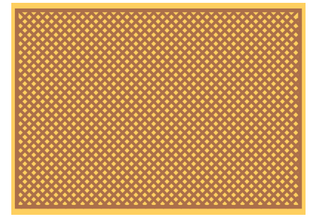
Cross-hatched reference plane in flex PCBs
Cross-hatched copper planes are used as reference planes in flex circuit boards. A cross-hatch plane is shown in the image below.
The ratio of cross-hatch conductor width (HW) to cross-hatch pitch (HP) plays an important role while characterizing the cross-hatch plane. If the ratio is about 0.293, 50% of the copper removal can be achieved. The lesser the ratio, the greater the percentage of copper to be removed. The only disadvantage of controlled impedance in flex is the requirement of having a higher controlled impedance value when compared to the rigid copper plane.
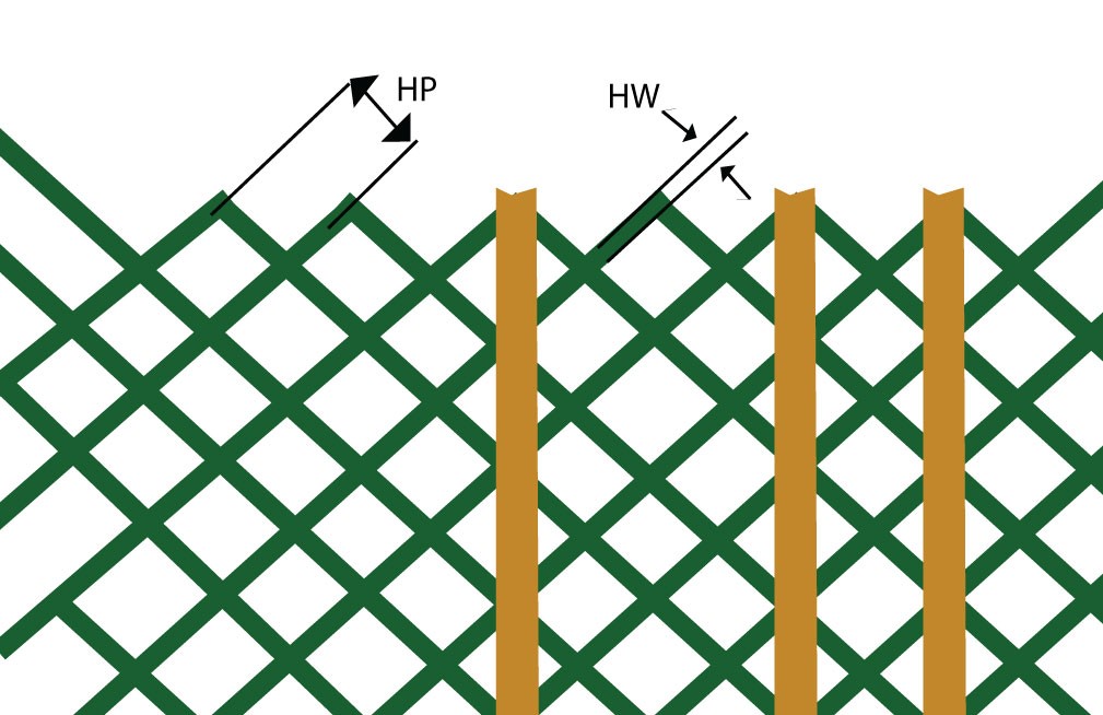
A cross-hatched reference plane means a significant percentage of copper is removed from the plane. This has a remarkable impact on controlled impedance in flex PCBs. However, cross-hatched planes don’t provide 100% shielding to the signal traces. The main purpose of cross-hatching the reference plane is to increase the flexibility of the circuit board.
Controlled impedance for rigid-flex boards
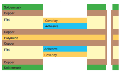
The above image shows a typical rigid-flex stack-up. As depicted, the flex layer (polyimide) is placed in the center of the stack-up. Therefore, the impedance traces in the flex layers need to change from microstrip (in the flex area) to stripline once they enter the rigid section. This may require thicker flex layer construction to meet the desired impedance value.
Read rigid-flex cuts electronic product assembly costs to learn how rigid-flex PCBs reduce the assembly expenses of an electronic device.
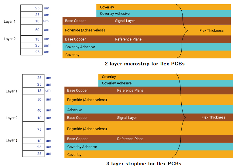
2-layer and 3-layer flex stack-ups for controlled impedance
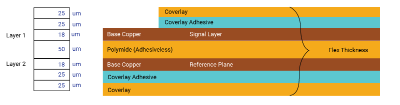
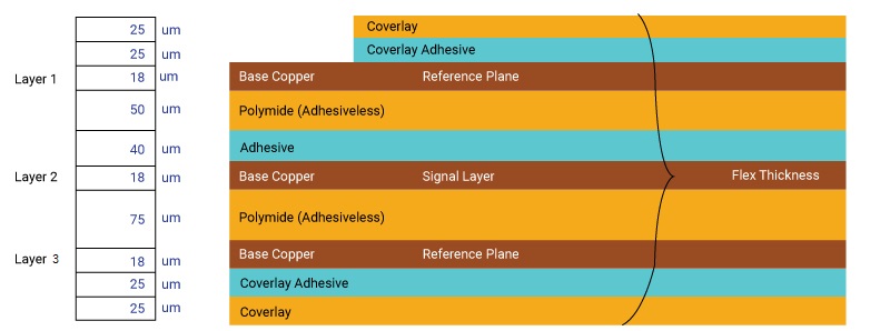
Impedance control in flex designs requires thicker flex cores than standard flex cores to achieve the desired impedance value. Thicker flex cores increase the overall thickness and reduce bendability.
The surface microstrip configuration allows for the thinnest possible flex core, offering the highest degree of flexibility. The stripline configuration allows shielding on either side of the traces. However, this configuration significantly increases the flex thickness, decreasing the flexing capability.
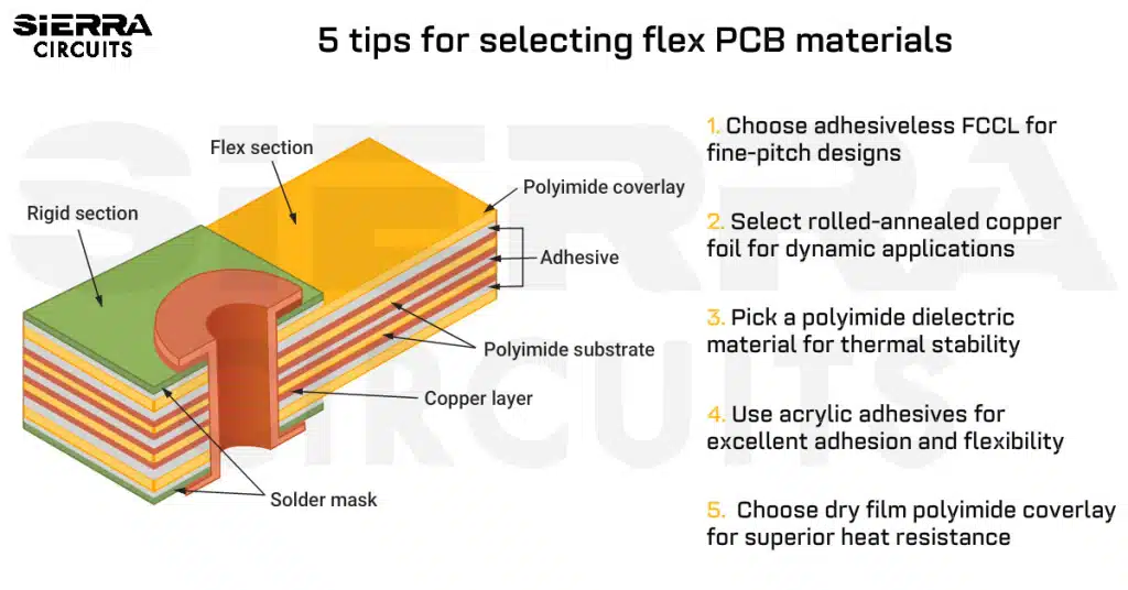
Flex PCB materials for controlled impedance
Flex boards are generally made of polyimide substrates. These substrates offer a lower Dk value (3 to 3.5) when compared to rigid materials. The thickness of the flex materials remains uniform throughout. This makes them ideal for flex-controlled impedance designs.
There are two types of polyimide materials: adhesive-based and adhesive-less materials. Both adhesive-less and adhesive-based materials can be used for the flex CI designs. However, due to their consistent results, adhesive-less materials are preferred for high-speed applications.
Advanced materials like Teflon and Teflon/Polyimide hybrids are suitable for high-speed applications. However, these materials are more expensive than polyimide materials. Standard adhesive-less polyimide materials fulfill the controlled impedance design requirements while reducing costs. Sierra Circuits uses Dupont materials for flex PCBs.
Controlled impedance is critical in minimizing signal reflections in a PCB. If you want to know more about controlled impedance for flex PCBs, let us know in the comments section. We will be happy to address your concerns.
Need assistance with your flex PCB design? Post your queries on our forum, SierraConnect, and our design experts will resolve them.

Flex PCB Design Guide
10 Chapters - 39 Pages - 45 Minute ReadWhat's Inside:
- Calculating the bend radius
- Annular ring and via specifications
- Build your flex stack-up
- Controlled impedance for flex
- The fab and drawing requirements
Download Now
About Milan Yogendrappa : Milan Y is an electronics and communication engineer with over 6 years of experience in developing and editing technical articles related to PCB design, manufacturing, and assembly. He is currently the editor-in-chief at Sierra Circuits.