


Contents

On-demand webinar
How Good is My Shield? An Introduction to Transfer Impedance and Shielding Effectiveness
by Karen Burnham
A solder mask is an insulation layer that covers conductive areas such as traces and pads. Inappropriate solder layer application may result in solder flowing towards undesired areas, leading to faulty electrical connections and corrosion. In addition to this, solder mask defects can also impact the signal integrity of your high-speed designs by modifying the impedance characteristics of the transmission line.
Knowledge of prevalent solder resist defects makes it easier to identify and rectify the solder mask errors during the design phase. You can avoid potential manufacturing errors such as short circuits, incorrect component placement, and weak solder joints.
In this article, you’ll learn:
- Common solder mask design errors
- Best practices to avoid solder resist issues
- How solder insulation errors impact the reliability of your PCB
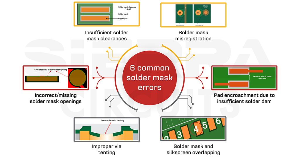
6 typical solder mask design errors
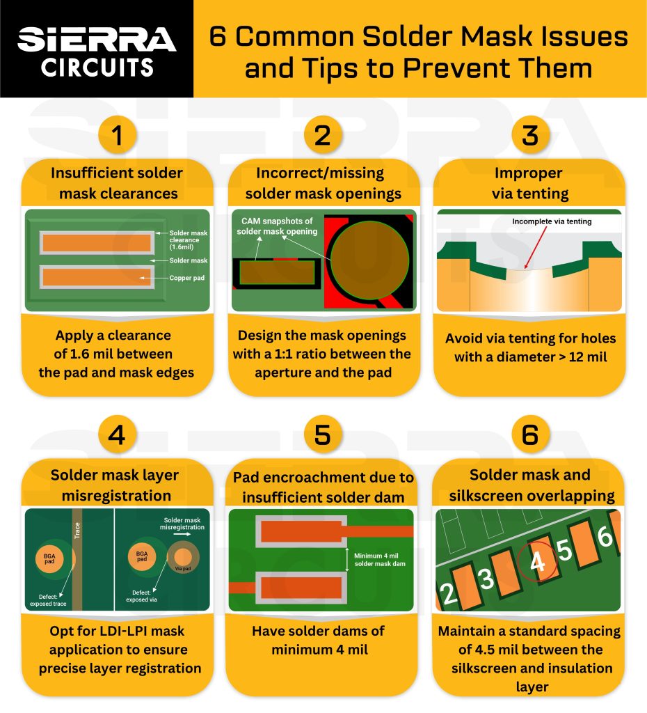
1. Insufficient solder mask clearances
Solder mask clearance around SMT pads decides how close the resist can be applied to the board surface features. This clearance defines whether a pad is solder mask defined (SMD) or non-solder mask defined (NSMD. To learn more, read solder mask-defined pads vs. non-solder mask-defined pads.

Missing or insufficient solder mask clearance can cause short circuits between adjacent pads. Conventionally, this clearance is half of the conductor spacing width. We recommend a clearance of 1.6 mil between the pad and mask edges.

2. Incorrect/missing solder mask openings
Solder mask opening refers to an area in which copper features are exposed to carry out the soldering process. If the apertures are small, the soldering flux residue gets trapped under the insulation layer. Larger exposure might lead to unwanted electrical connections and damage to the circuit.
To avoid this defect, design the mask openings such that the ratio between the aperture and the respective pad is 1:1. To learn more, read IPC-J-STD-001 soldering requirements.

3. Improper via tenting
Tenting is a process of covering vias with an insulation layer. This technique prevents the plated holes from being exposed to hazardous chemicals, which in turn leads to solder wicking. Inadequate tenting might expose the vias and lead to solder bridges.

Tenting works well on the small vias with less than 12 mil finished hole diameter. Always tent the vias on both sides to increase the via reliability. This rule is not applicable to via-in-pads and vias on ground pads. These holes require exposed copper on one side. Therefore, implement tenting on another side for such instances.
Via tent may crack or leave a void if the via diameter is too big (>12 mil). Consequently, these solder voids allow hazardous impurities to enter the via barrel. This results in reliability issues. In such cases, leave the vias untented with an opening of pad size +1.6 mil and ensure appropriate plating. For instance, if your pad size is 30 mil, the solder mask opening should be 31.6 mil. See via filling techniques designers need to know.
4. Solder mask layer misregistration
Solder mask misregistration occurs when the insulation layer is not accurately aligned with the underlying copper traces and pads. Incorrect pad dimensions, resist opening, and inappropriate solder mask thickness contribute to misregistration issues.
To avoid alignment issues, we use a minimum of 0.5 mil mask thickness. If you require a thicker resist area, you can mention the same in your PCB fab notes. However, excessive resist application may cause serious damage to soldering joints and hamper your PCBA.

5. Pad encroachment due to insufficient solder dam
Solder dam refers to the barrier between two mask openings of the adjacent conductive features. This dam ensures correct electrical insulation and also restricts solder flow only to the designated pad.

If the dam is too narrow, it might not be effective in preventing solder bridging. If it is too wide, it might lead to insufficient solder coverage on the pad. Incorporate a minimum of 4 mil solder dam to prevent pad encroachment.

Design for Manufacturing Handbook
11 Chapters - 96 Pages - 90 Minute ReadWhat's Inside:
- Annular rings: avoid drill breakouts
- Vias: optimize your design
- Trace width and space: follow the best practices
- Solder mask and silkscreen: get the must-knows
Download Now
6. Solder mask and silkscreen overlapping
Mask openings are intentionally kept slightly larger than the corresponding pads to ensure proper coverage and prevent solder mask slivers. This extension can lead to the resist layer partially covering the silkscreen markings of surrounding pads. Furthermore, inappropriate text clearance from the solder mask causes the silkscreen to overlap with the adjacent text or pad.
To avoid this error, maintain 4.5 mil of standard spacing between the silkscreen text and the insulation layer.

Key takeaways for PCB designers
- Insufficient solder mask clearances can lead to short circuits between adjacent pads
- Do not tent the large vias (pad diameter above 12 mil) as it can lead to solder voids and reliability issues
- Inappropriate mask openings can result in unwanted electrical connections and damage to the circuit
- Implement a minimum of 4 mil solder dam to prevent pad encroachment
6 design tips to prevent solder resist issues
To evade solder mask errors and ensure a successful PCB manufacturing process, follow these guidelines during the design phase.
1. Include solder mask expansions
Avoid designing extremely small solder mask openings, especially for HDI boards. Add solder mask expansions around the copper pads to provide a buffer zone and ensure sufficient coverage. This expansion compensates for any misalignment during the manufacturing process.

2. Validate all the solder mask features during the DRC process
Run a design rule check to verify the mask clearances, openings, and solder dam dimensions. Always be aware of your CM’s capabilities and ensure that your design is within their specs.

3. Adhere to the DFM rules
Stick to the DFM guidelines to ensure proper solder mask application and avoid potential solder mask manufacturing errors. Validate dimensions of solder mask clearance, openings, web, layer registration, and expansions before submitting your PCB design files.
Use our Better DFM tool to automatically optimize your solder mask features. This advanced PCB design tool will automatically increase or decrease the solder resist clearances to maintain the required spacings.
4. Set the correct design constraints for clearance
Maintain appropriate clearances and spacings between solder mask features, such as solder pads, vias, and traces. Perform thorough reviews and tests to ensure error-free Gerber files. Maintain clear design documentation of your design, solder mask specifications, and communicate your requirements to the manufacturer.
5. Verify the footprint dimensions with the datasheet
Double-check the accuracy of component footprints. The solder mask openings should align correctly with the respective pads. Pad dimensions and shape should match the component datasheet. If there are any discrepancies, it leads to various solder mask errors discussed above.

6. Opt for an LDI (laser direct imaging) mask finish for HDI boards
When your board has tight spacing constraints and the mask clearance is narrow around the SMT pad, opt for an LDI-LPI solder mask finish. This coating is semi-glossy in nature and involves better precision than others.
How masking issues impact the circuit board’s reliability
Defective solder resist layers can significantly affect the durability of your PCB. It leads to various alarming issues such as:
1. Solder bridges
A solder bridge is an unintended electrical connection between two solder pads/pins on a PCB. Excessive resist applied to the pads can ooze between the pads and create a solder bridge. This can lead to malfunctioning circuits.

2. Solder mask slivers
Slivers are thin, unintended areas of insulation material that remain between adjacent pads or traces. They occur due to inadequate spacing between adjacent copper features. As a result, slivers reduce the solderable area on the pads and hamper the PCB assembly process.

3. Solder mask pinholes/voids
Pinholes are tiny voids in the solder mask layer. If the solder resist is not applied correctly, it can leave gaps between the pads and allow the solder to flow. These voids can lead to exposing copper traces to oxidation.

4. Degradation of conductive features
Solder barrier errors compromise the circuit protection against hazardous contaminants. Voids in the mask layer allow moisture and corrosive agents to reach the underlying copper features, leading to degradation.
5. Lower manufacturing yield
Incorrect mask application can result in weak solder joints and reduced mechanical strength, leading to misalignment and tilted components. Hence, to fix these issues, the board should undergo respins, increasing the production cost and lowering the yield.

PCB Design for Assembly Handbook
6 Chapters - 50 Pages - 70 Minute ReadWhat's Inside:
- Recommended layout for components
- Common PCB assembly defects
- Factors that impact the cost of the PCB assembly, including:
- Component packages
- Board assembly volumes
Download Now
Solder resist issues can significantly impact the reliability of your PCB. To avoid these defects, you need to provide appropriate mask clearances and openings. Adhere to your CM’s DFM guidelines to rule out potential manufacturing errors.
Effective communication with your CM ensures good mask coverage, resulting in reliable board performance. If you have any design queries related to the solder mask, feel free to comment below.

About Poulomi Ghosh : Poulomi is a microwave engineer specializing in EMI, EMC, RF, and high-speed electronics. As a senior technical writer at Sierra Circuits, she creates advanced engineering articles and webinars for hardware engineers and PCB designers.


Start the discussion at sierraconnect.protoexpress.com