


Contents

On-demand webinar
How Good is My Shield? An Introduction to Transfer Impedance and Shielding Effectiveness
by Karen Burnham
Flex PCB design requires a slightly different approach than rigid PCBs. While designing a flex board, you must consider the board outline, bending requirements, optimum material selection, stack-up, placement of copper features, and cost factors.
A well-designed flex PCB will be lightweight, robust, durable, reliable, and easy to install. Hence, it suits demanding applications like aerospace, satellites, IoT, medical, and wearable devices. Flex boards offer improved endurance to vibrations and high temperatures, making them more sustainable against harsh environmental conditions.
Flex PCBs can significantly save manufacturing costs, reduce space consumption, and be lighter. However, their design must be optimized for their materials and use cases. This article provides several useful pointers to ensure maximum reliability, manufacturability, and economy when planning your first flex printed circuit.
Before we begin with the flex design essentials, look at our infographic 5 design guidelines to build a reliable flex PCB. This can be your visual guide to craft a reliable circuit board.

1. Understand the bendability of your flex PCB
The flexibility feature of flex PCBs enables designers to implement them in tiny packages. It is vital to understand two things about bendability: how many times the board will flex and to what extent it will flex. The number of times it can bend determines whether the PCB will be static or dynamic. A static board is considered bend-to-install and will flex less than 100 times in its lifetime. It is generally bent during the assembly process. A dynamic board‘s design needs to be more robust in nature, as it flexes regularly and will need to withstand tens of thousands of bends.
The thickness of these boards depends on several factors:
- Dielectric material selection
- Copper layer count
- Base copper weight
- Adhesive thickness
The bend radius is the degree to which the flex area of a circuit board can flex. The minimum angle at which the flexible region can bend must be identified early in the design phase. This ensures that your design allows the necessary amount of bends without damaging the copper. It is calculated based on the number of layers in the PCB.
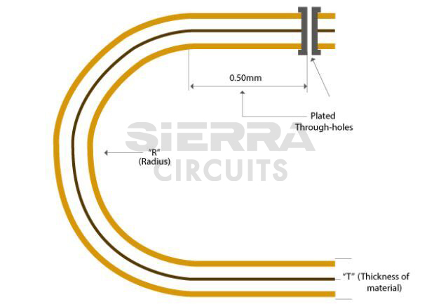
The bend ratio is the ratio of the bend radius (R) to the thickness (T) of the flex circuit. The failure probability is higher if the bend radius is tighter. For a reliable flex PCB design, the minimum bend ratio for different types of circuits according to IPC is mentioned in the table below:
| Number of layers | Bend ratio for static boards | Bend ratio for dynamic boards |
|---|---|---|
| Single layer | 10:1 | 100:1 |
| Double layer | 10:1 | 150:1 |
| Multilayer | 20:1 | Not recommended |
Design tips when laying out the bend areas:
- Avoid 90º bends as that causes high strain. Use gradual and large curved angles that prevent circuit damage.
- Plated through-holes and the placement of components should be avoided in the bend area.
- Conductors running through a bend area need to be perpendicular to the bend axis.
- Stagger conductors in multi-layered circuits for greater circuit effectiveness.
- Place conductors smaller than 10 mils within the neutral bend axis where there is the least tension or compression during flexing.
The thickness of the flex circuit directly influences its flexibility. The lower the thickness, the more the pliability. Reducing copper trace thickness can increase bendability. It becomes difficult for the board to bend in multilayer flex PCBs with a large layer count. Copper thickness can be reduced by cross-hatching the ground planes on both sides of the signal layers.
The tighter the bend radius, the higher the flexibility. However, the chances of damage are also higher. You should understand the optimum trade-off between having a smaller radius and the extent of bending required for your flex PCB design.
If there are no traces in the bend region, the bend radius can be minimized by inserting cutouts or slots. Using cutouts will reduce the amount of material required to bend. Another option is removing sections of the flex where there is no circuitry, although this must be removed lengthwise and will require routing afterward.
Flex PCB Design Guide
10 Chapters - 39 Pages - 45 Minute ReadWhat's Inside:
- Calculating the bend radius
- Annular ring and via specifications
- Build your flex stack-up
- Controlled impedance for flex
- The fab and drawing requirements
Download Now
2. Know your flex PCB materials
IPC 4202, 4203, and 4204 standards prescribe different materials and their specifications. You need to know the PCB materials and the characteristics that suit your design criteria. The properties that you need to consider are:
- Moisture absorption
- Fire retarding
- Dielectric constant (Dk)
- Glass transition temperature (Tg)
- Coefficient of thermal expansion (CTE)
Read IPC standards for laminate selection to know more.
Basic flex materials
Flex materials offer better material properties than rigid PCBs. A flex board will have the following materials:
Dielectric insulator and coverlay: Polyimide is used primarily for flex core and coverlay layers. The thickness of this dielectric flex material is uniform, with an improved dielectric constant (Dk) value ranging between 2.5 and 3.2 at 10 GHz. The lack of woven glass reinforcement eliminates variations in Dk. Due to its cast manufacturing process, polyimide has an extremely uniform thickness. The typical layer thickness ranges from 0.5 to 4 mils.
Conductor: Copper foil is a good conductor, so it is extensively used in making PCB circuits. Polyimide flex cores are clad with either electro-deposited or rolled annealed copper. This copper is very thin and suitable for both dynamic and static applications. 0.5oz (0.7 mil) copper is commonly used in flex PCBs. The most common flex PCB copper weights are 0.5oz and 1oz. The maximum copper weight is 2oz. This gives the best combination of the thinnest possible construction.
Flexible copper-clad laminate (FCCL): It is a flex PCB’s core component comprising copper foil and polyimide layers. These boards generally use rolled annealed copper. Rolled annealed copper is created by subjecting electro-deposited copper to the rolled annealed process. It provides a tighter bend radius. The grain structure is transformed from a vertical to an elongated horizontal structure. This improves the ductility of copper, making it suitable for dynamic applications. Fully annealed or low-temperature annealed copper gives better flexing characteristics.
Bondply: These composites are polyimide films coated with B-staged acrylic adhesives on both sides. To encapsulate etched details in heavy copper multi-layered constructions of flex/rigid-flex boards, bondply is used between two conductive layers from different FCCL cores.
Adhesives: Different types of adhesives are available for flex circuits—acrylic adhesives, epoxy adhesives, and pressure-sensitive adhesives (PSA) are a few of them. PSAs are flexible, have superior bond strength, and are easy to work with. They can adhere to the substrate or other surfaces directly. PCB adhesives can be acrylic or epoxy-based and supplied as flexible tape.
They are known as thermosetting adhesive films. Applying enough pressure and heat makes the film tacky to secure the components. After this, they are placed in an autoclave/pressure, and additional heat and pressure are applied to finalize the bond.
Acrylic adhesives stay malleable even after they are cured and are a good choice for dynamic applications. Epoxy adhesives are not preferred for dynamic operations as they cure hard. In a rigid-flex PCB design, the flexible region can use acrylic adhesive, and the rigid region can use epoxy adhesives.
Stiffeners: Single-sided, double-sided, and multilayer flex circuits can be stiffened in specific areas by adding localized rigid material called PCB stiffeners. This can add mechanical support for mounting components, increasing strength, thickness, and rigidity. Kapton and FR4 materials are commonly used for stiffeners.
Sometimes, aluminum or stainless steel is used. These materials can be attached with thermally cured acrylic adhesive or pressure-sensitive adhesives. Stiffeners can relieve strain, balance weight, and promote heat dissipation. They reinforce solder joints and increase abrasion resistance.
Surface finish types: Many different types of surface finishes provide a solderable surface and prevent copper oxidation. Based on the application, choose what best suits your flex PCB. The board surface is protected using coverlay, covercoat, photo-imaged dry film, and liquid photo-imaged polymer.

Consider the placement of preliminary components (SMT or TH) and determine whether those components require stiffeners. Circuitry layout makes or breaks a PCB. Important layout design and routing considerations during flex PCB design include:
- A large bend radius is preferable to sharp angles that shorten a board’s lifespan.
- Curved traces cause lower stress than angled ones.
- Conductors should also be routed perpendicular to the overall bend. This eliminates the stress points that can cause trace copper breakage.
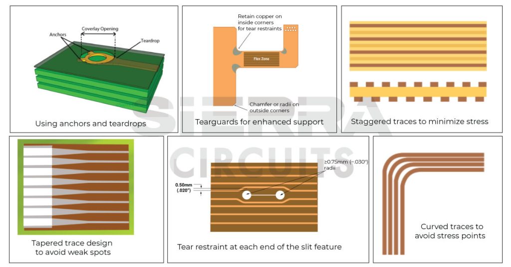
- Stagger traces on the top and bottom of a flex board with two or more layers. This will avoid I-beaming due to stacked copper traces, which minimizes the stress that can damage copper circuits.
- Use tear guards in the circuit to reinforce the flex material along the inside bend radius and eliminate tears.
- Transition gradually from wide to narrow traces, always tapering down the traces from the thick to the thin.
- Avoid discontinuities like vias, cut-outs, slits, and holes in the bend area. Bending a via causes stress and cracks that ultimately cause malfunctions and failures.
- Terminate cutouts/slits in flex region as per IPC standards with circular sections (relief holes) to prevent tearing at corners. The radii should be greater than 0.75mm.
- Use stiffeners in areas susceptible to excessive pressures. Anchors and spurs encapsulated with coverlay should be used to avoid trace lifting and pad peeling.
- Always keep special copper features and vias, and plated through holes 50-60 mil away from the transition region of a rigid-flex PCB. The region in between the flex and the rigid portion of a rigid-flex board is called a transition zone.
- Flex materials are prone to more movement and contraction during manufacturing. This makes drill-to-copper distance a crucial factor while designing your flex board. Always have the drill-to-copper distance of at least 8 mil.
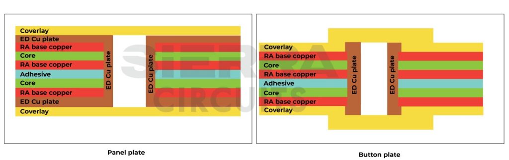
- Understand if panel plating or pad-only plating (button plating) is preferable for your flex circuit. Copper is deposited only on the vias/pads in button plating. Due to the smaller amount of copper needed, button plating provides more flexibility. It allows manufacturers to control the copper thickness and improve etch yields in small etch patterns. It also facilitates controlled impedance at higher speeds as conductor traces have consistent copper thickness, width, and spacing. It is expensive due to extra processing steps.
For more flex design tips, see avoiding the common errors in flex PCB design.
Via design considerations in flex boards
It is important to understand the risks of using vias when designing flex boards. Vias can crack or break in flex designs.
To mitigate this risk:
- Use teardrop (pad fillets) shaped vias to connect traces or through holes in flex boards. This reduces potential stress concentration points. Fillets are appropriate when the pad diameter is larger than the width of the connecting strand.
- Keep the annular rings as large as possible. Their main purpose is to establish a good connection between the via and the copper trace. The minimum annular ring should be 8 mils for a flex PCB.
- Vias are okay over a stiffener, but vias just off the edge of a stiffener are at risk of cracking.
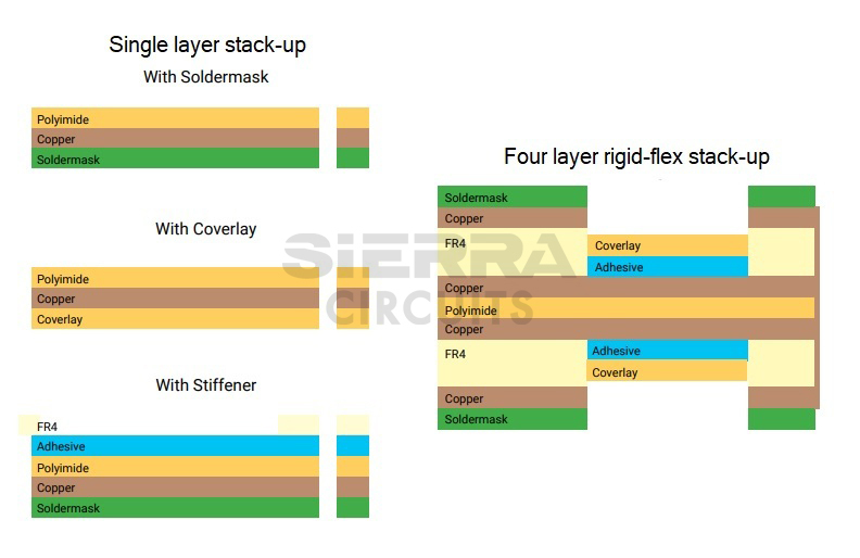
4. Select a suitable flex PCB stack-up
Optimizing your flex stack-up by considering the type of application (static/dynamic), bend radius, number of layers, and overall board thickness. Consider these guidelines when designing the build-up:
- Build flex board models early in the design phase using stiff paper or Mylar. Virtual mock-up models can be built using CAD tools. You can then glue the rigid sections to this using cardboard and put on the primary components. This model should fit your required form.
- Choose your materials based on this design and operating environment.
- While designing a rigid-flex board, place flexible layers in the middle to avoid slippage.
- Always implement an even number of layers to ensure a balanced stack-up.
- Mention the thickness and impedance requirements of each layer in your build-up.
- Choose industry-standard ECAD/MCAD tools that offer a complete toolset for designing, laying out, and customizing stack-up in flex/rigid-flex board features.
- Incorporate the air-gap construction method for rigid-flex PCBs to eliminate the use of flex adhesives within the rigid sections, addressing reliability issues via
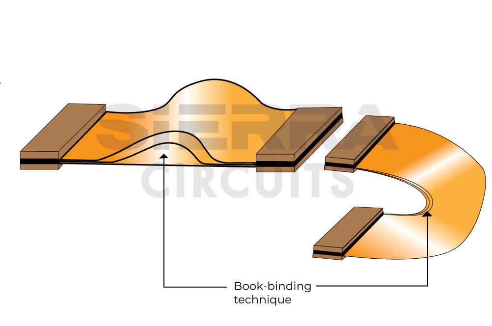
In high-layer count PCBs, the circuit bookbinding technique enables multilayer flex to bend in a small radius without deforming. This method is expensive but has several advantages:
- Reduces stress experienced by circuit layers, increasing shelf life.
- Compatible with all mounting processes.
- Prevents the inner layers from buckling at the bend radius.
- The board can perform bends of 180º.
- It can be used in critical high-density applications.
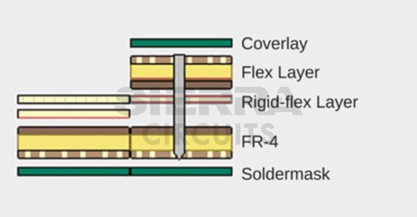
Sierra Circuits’ rigid-flex manufacturing process is as follows:
Step 1: Process the flex layer as a two-layer flex board.
Step 2: Laminate the flex layers between the rigid layers.
Step 3: Mill the layers so the flex becomes visible.
Putting flex layers inside the stack-up protects from exposure to outer-layer plating. This placement also simplifies manufacturing and improves impedance and control in the flex area. The flex layer can be etched away from the design as part of a separate process, allowing for more protection.
To design better flex PCBs with Vern Solberg’s expert pre-layout tips, read flex PCB design guidelines part 1: pre-layout considerations.
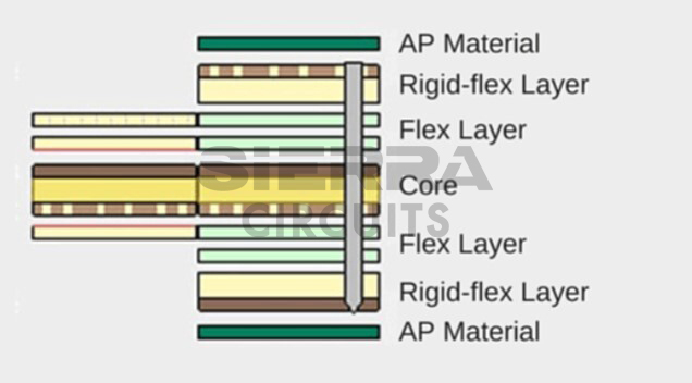
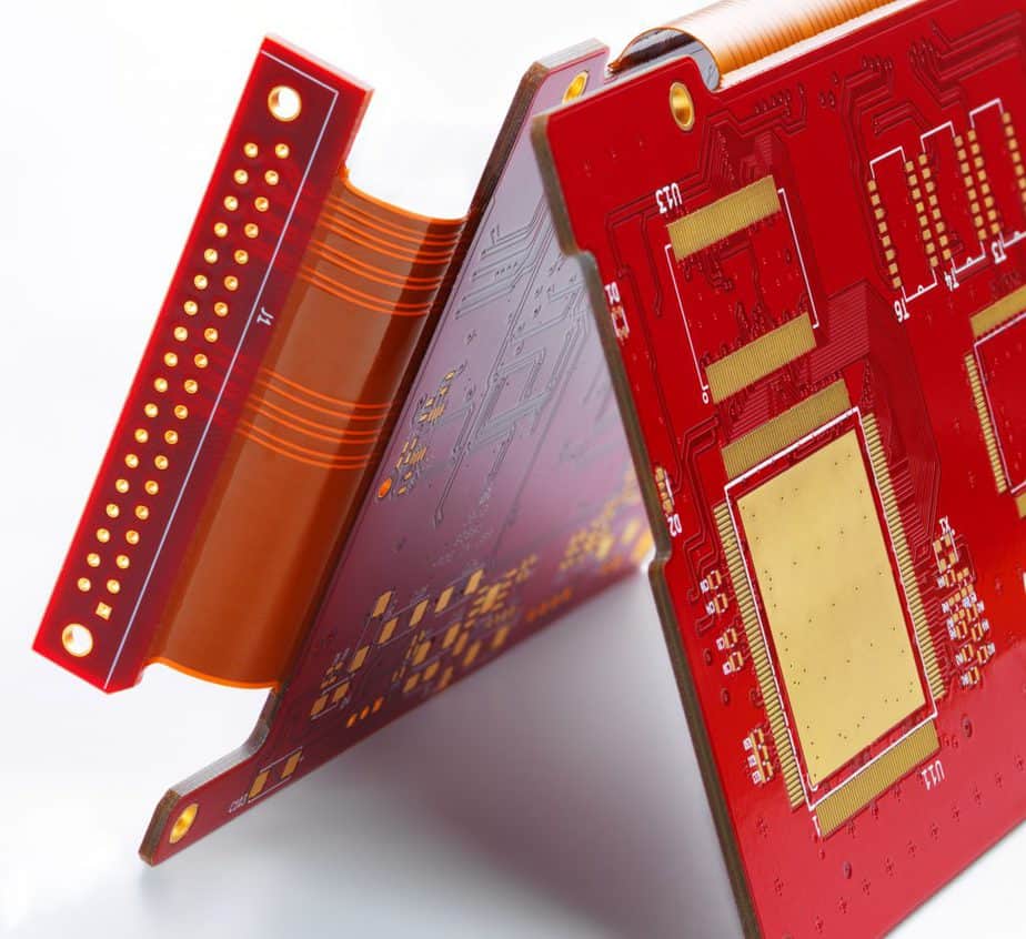
Flex PCB stack-up design case study
This was a four-layer flex board with ZIF connectors requiring controlled impedance. The flex layers were located on the outside of the stack-up, which increased the possibility of manufacturing issues. There was also difficulty in achieving impedance requirements.
The solution
We embedded the flex layers in the center of the stack-up, as shown in the figure below. This protected the layers during manufacturing and ensured that the less-durable flex layers were not exposed to outer-layer plating. This is how most rigid-flex stack-ups are designed. Panels are harder to handle and process when the flex layers are outside. This made the board more durable and easier to manufacture. It also allowed for better impedance and control around the flex finger area.
Keeping the rigid material on the outside also allows us to manufacture what is essentially a rigid panel. The flex layers are protected by surface plating. However, it can cause embrittlement (brittle fracture), and the process must be carefully controlled to prevent it.
The material also played a large part in making this board rigid-flex instead of flex. Rigid AP (adhesive-less/high-performance) material was used to improve impedance and reliability. It was a much better option than the original FR-4 material.
To learn how our designers reverse-engineered a flex PCB to create design files, see our case study on reverse-engineering a flex PCB to generate design files.
Controlled impedance and EMI shielding
Impedance control is required in flex stack-ups to reduce signal reflections and achieve dependable signal integrity. When designing your board, you must understand how to build a flex stack-up with controlled impedance, especially for high-speed applications.
Use EMI/RFI shielding techniques in your flex circuit to reduce noise. Controlled impedance and bend requirements are two factors to consider while selecting shielding methods. It is achieved using copper layers, silver inks, or specialized films. The shield(s) must have electrical properties that meet reference plane criteria and EMI to obtain regulated impedance values.
Solid copper shield layers provide better shielding but less flexibility. Cross-hatched copper layers are more flexible due to reduced copper but may not provide effective shielding. Tighter meshes provide better isolation and reduce emissions. These shields are connected to the ground via stitching in the flex area, which is a drawback. Design your circuit board by negotiating all these parameters. This shielding technique supports controlled impedance designs.

Controlled Impedance Design Guide
6 Chapters - 56 Pages - 60 Minute ReadWhat's Inside:
- Understanding why controlled impedance is necessary
- Stack-up design guidelines
- How to design for impedance
- Common mistakes to avoid
Download Now
5. Follow IPC design, manufacturing, and testing standards for flex PCBs
Testing is essential in ensuring the integrity of your flexible printed circuit boards. To verify the quality of your raw materials and finished products, we adhere to IPC standards for testing flex PCBs, such as IPC-6013, IPC-2223, and IP-FC-234, and their respective successors. Considering these standards, the flex boards can be tested for efficiency and performance.
IPC-2221 (Generic standard on printed board design)
IPC-2221 establishes the generic requirements for PCB designing, along with other forms of component mounting and interconnecting structures. This document also provides the test coupon design standards used for quality conformance testing for different board parameters.
IPC-2223 (Sectional design standard for flexible / rigid-flexible printed boards)
This document is used in tandem with the document IPC-2221. IPC-2223 establishes the design specification of the flex and rigid-flex PCBs, component mounting, and interconnecting structures. It guides in many design areas, such as material selection and construction, plating, conductor bend considerations, capacitance, and impedance control. It gives information on unsupported edge connectors/fingers specifications, using dual/single ZIF connectors and dielectric thickness adjustment between rigid and flexible regions.
Read IPC-2223 standards and design violations for rigid-flex boards to understand common design violations and ways to prevent them in rigid-flex PCBs.
IPC-FC-234
This document provides information regarding the use of pressure-sensitive adhesives (PSAs) to assemble flex PCBs. This guide provides information on available adhesive types and suggested processes for their proper use. It highlights strengths, weaknesses, limitations, and the processes needed to create proper assemblies/bare boards.
Circuit board testing is an application and environment-specific process. For example, aerospace and space applications require a more formidable process than consumer-oriented applications.
IPC-6013
The IPC-6013 standard provides the qualifications and performance specifications for flex PCBs. The current version is IPC 6013E, published in 2021. This standard supersedes several previous IPC standards, including the original IPC-6013 from 1998. It specifies many different test methods for flex PCBs, including thermal, bend, and impedance testing. This standard also includes quality assurance provisions such as sample test coupons, guidelines for acceptance, and quality conformance tests.
IPC-600
This standard specifies the acceptability criteria for all rigid, flex, and rigid-flex board classes through visual interpretations. It illustrates the negotiable and non-admissible conditions externally or internally observed on the manufactured flex boards. The latest version is IPC 600 K, which was released in 2020.
IPC-A-610 and IPC/ EIA J-STD001
IPC-610 is the standard for the acceptability of PCB assemblies, including flex/rigid-flex boards.
IPC/EIA J-STD001 standard gives soldered electrical and electronic assembly requirements.
6. Know the factors that affect the cost and turn-time of your flex PCB
While designing a flex board, the goal should always be to create a cost-effective product without sacrificing performance. The major cost-driving factors in a flex PCB design are:
- Board size and shape
- Materials
- Number of layers
- Dimensional tolerances
- Circuit construction type
- PCB grade (class)
- Thickness of the copper foil
- Size of drill holes
- Drill to copper distance
- Surface finish requirements
- Via features
- Types of stiffeners
- Plating requirements
Remember these considerations and common DFM mistakes in flex during the design phase of your project. Always consult your CM’s engineering team for the best possible design advice.
The five important factors that delay the turnaround time of flex boards are:
- Inappropriate bend requirements
- Incomplete design data requirements
- Design-related issues
- Missing ZIF connector specification
- Lack of information on flex-to-rigid transition zones
For on-time delivery of the flex boards, you must ensure that you provide all the necessary information to your manufacturer and follow standard design specifications. Your fab drawing for flex-PCBs should not have any missing details. Information on flex materials, stack-ups, dimensions, flexibility, plating, marking, and testing requirements should all be mentioned without fail. Rigid-flex fab notes must consist of rigid notes and flex notes separately.
For a detailed explanation, see the 5 factors that delay flex PCB quick turn delivery.
7. Choose a competent flex PCB manufacturer
When it comes to flex PCB design, you must choose the right manufacturer to provide the support you need. Make sure that the PCB shop you pick produces flex circuit boards regularly. Ensure that they produce high-quality, quick-turn PCBs. Do not hesitate to ask about the materials they use, surface finish types, and technologies they implement.
Know your PCB supplier’s capabilities. They have their own design rules and recommendations that should be considered. Based on your circuit density and line spacing, they might suggest changes in layout design for an effective design solution. Read our case study on routing a microcontroller and BGA in rigid-flex PCBs to learn how we successfully routed a BGA and a microcontroller using the via-in-pad technique.
Consult with them to ensure that all the DFM guidelines for flex and rigid-flex are followed. This prevents errors and delays in the flex prototype. You can request a stack-up before designing begins.
Work with your board supplier during material selection as well. The material should be suitable for your operating environment.
Flex PCB assembly can be challenging as the boards are not sturdy. Specialized fixtures should be created to hold them for an easy assembly process. You must ensure the manufacturer removes all the moisture before the flex circuit is subjected to high temperatures. Flex circuits must be processed immediately after pre-baking or right after fabrication to address common design challenges in high-temperature flex PCBs. Be aware of the advanced assembly and testing equipment your manufacturer uses.
Make sure that your manufacturer has the necessary certifications and registrations. They should also be able to give you a higher quality-to-cost ratio. It is even better to visit your PCB manufacturer and see their capabilities for yourself. Always choose turnkey PCB manufacturing and assembly from a single facility to avoid multivendor miscommunication.
If you come to Sierra Circuits, we will give you a “behind-the-scenes” tour of our facilities in Sunnyvale, CA. You will learn everything you need about our manufacturing and assembly process.
Flex and rigid-flex boards are proving their worth in innumerable applications across the globe today because of their intrinsic advantage. However, they do require careful design consideration and collaboration with your fabrication partner. Let us know in the comments section if you need assistance building your flex PCB. Our design and manufacturing experts will be happy to help you.
About Amit Bahl : Amit Bahl, widely recognized as the PCB Guy, earned his Bachelor of Science in Engineering from UCLA. He is currently the Chief Revenue Officer at Sierra Circuits, where he continues to lead efforts to simplify the PCB design journey and support designers and engineers in creating high-quality boards.


Start the discussion at sierraconnect.protoexpress.com