Advanced Practices in HDI PCB Design

Amit Bahl
Director of Sales & Marketing
Sierra Circuits
Fill out the form:
In this webinar
Efficient routing strategies to breakout chips and BGAs and fine lines that transmit signals efficiently are what come to mind when designing HDI PCBs. The primary objective is to furnish these advanced capabilities in a small package. To achieve this, a designer should be aware of the progressive design aspects of high-density interconnect technology. Join us to learn the cutting-edge techniques that enable you to design an efficient HDI circuit board.
What you will learn:
1. A quick glance at HDI PCBs
2. Best design practices in HDI
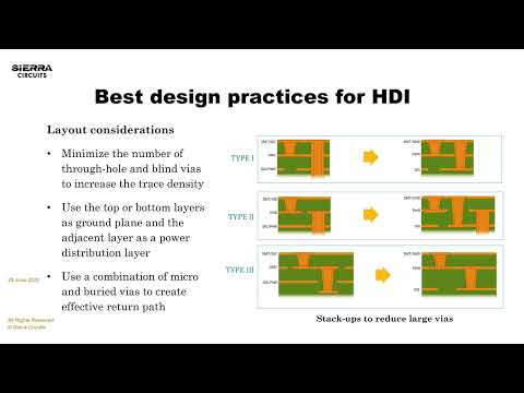
a. Reducing the big through-hole vias
b. Layer stack-up
c. Benefits of using blind via
d. Smaller traces/spaces and vias/pads
e. Material considerations
f. Aspect ratio
g. Material types by reinforcement
h. Stack-up considerations
i. ELIC stack-up
j. Microvia sizing
k. Sequential lamination
l. Controlled impedance constraints
m. Split power/ground planes with HDI
3. Signal integrity for HDI
4. BGA breakout in HDI
5. Advanced routing strategies
a. Via-in-pads
b. Dogbone fanout
c. Boulevard structures
6. IPC standards for HDI
About Amit Bahl
Amit has been in the PCB industry for 20 years. He is the Director of Sales and Marketing at Sierra Circuits. His passion is to empower tech companies to achieve their visions and change the world. Rockets going into space, self-driving cars taking up the streets, cancer-fighting medical devices, protecting the country, he’s ready to build any circuit board!
Watch the Trailer