Speak to an Account Manager
![]() +1 (800) 763-7503
+1 (800) 763-7503
Related Categories — KiCad Tutorials » PCB Design
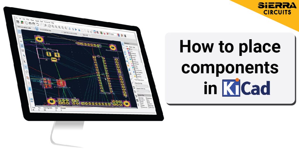
How to Place Components in KiCad
In our previous tutorial, we demonstrated how to set up design rules in KiCad, which included how to create a netlist and how to import it to the board file. Today, we will show you how to place components in KiCad. We will also cover how to define your PCB outline.
KiCad Tutorials
How to Create a Schematic for High-Speed Designs in KiCad
KiCAD is a widely used free Electronic Design Automation (EDA) software. The software is mainly used as a ... more »
High Speed
KiCad Version 9: Exploring the New Features
KiCad is an open-source software that offers PCB designers and hobbyists a free yet powerful alternative to commercial ... more »
KiCad Tutorials
How to Place Components in KiCad
In our previous tutorial, we demonstrated how to set up design rules in KiCad, which included how to ... more »
KiCad Tutorials
How to Create a Schematic for High-Speed Designs in KiCad
KiCAD is a widely used free Electronic Design Automation (EDA) software. The software is mainly used as a ... more »
High Speed
KiCad Version 9: Exploring the New Features
KiCad is an open-source software that offers PCB designers and hobbyists a free yet powerful alternative to commercial ... more »
KiCad Tutorials
How to Route Differential Pairs in KiCad
Routing is simply the process of wiring between the components placed in the PCB design while following all ... more »
KiCad Tutorials
PCB Component Footprint Creation in KiCad, Altium Designer, and Allegro
Components that need to be assembled on a PCB will have designated locations according to the design. Footprint ... more »
KiCad Tutorials
How to Export Production Files in KiCad: IPC-2581 and Gerber
In this tutorial, we will study how to export Gerber files and other production files in KiCad. To ... more »
KiCad Tutorials
How to Route a PCB in KiCad
We selected an 8-mil track width and spacing for the differential pair. But this needs to be done ... more »
KiCad Tutorials
How to Create a Schematic and Symbol Library in KiCad
In this KiCad tutorial, we will explain how to create a schematic and a symbol library for components ... more »
KiCad Tutorials
Try the KiCad Plugin for an Instant PCB Quote
Get instant PCB fab and assembly cost estimation for your designs through Sierra Circuits’ KiCad quote plugin. You ... more »
KiCad Tutorials


Fabrication, Procurement, & Assembly. PCBs fully assembled in as fast as 5 days.
- Bundled together in an entirely-online process
- Reviewed and tested by Engineers
- DFA & DFM Checks on every order
- Shipped from Silicon Valley in as fast as 5 days

Fabrication. Procurement & Assembly optional. Flexible and transparent for advanced creators.
- Rigid PCBs, built to IPC-6012 Class 2 Specs
- 2 mil (0.002″) trace / space
- DFM Checks on every order
- 24-hour turn-times available

Complex technology, with a dedicated CAM Engineer. Stack-up assistance included.
- Complex PCB requirements
- Mil-Spec & Class 3 with HDI Features
- Blind & Buried Vias
- Flex & Rigid-Flex boards