Contents

On-demand webinar
How Good is My Shield? An Introduction to Transfer Impedance and Shielding Effectiveness
by Karen Burnham
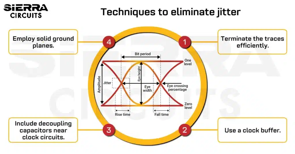
Just like trace impedance, via impedance is also important in maintaining the signal integrity of your PCB design. At high frequencies, vias behave as the breakpoints along the transmission line and disrupt the impedance continuity. This causes signal reflections and introduces jitters in the signal path.
Via impedance mainly depends on the physical dimensions of the via barrel, pad, and anti-pad. By regulating these characteristics, you can control the signal reflections. In this article, you will learn the significance of via impedance and solutions to mitigate the odd effects of impedance discontinuity caused by a via.
What’s the importance of via impedance?
Via impedance doesn’t matter as long as the signal transmission happens at low frequencies. At high frequencies, the vias introduce impedance discontinuity and result in signal reflection.
The magnitude of this reflection depends on the difference between the two impedances (i.e. impedance of the trace and impedance of the via at the transition point).
The signal reflection affects the controlled impedance and impacts the board’s functionality. This is mainly due to parasitic capacitance and parasitic inductance. In the next section, you will see how these parasitics affect the impedance of a via.
Effect of parasitic capacitance and parasitic inductance on via impedance
Parasitic capacitance increases the signal transmission time
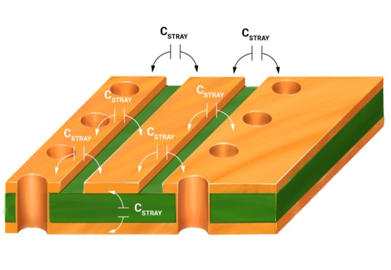
Parasitic capacitance is a result of the virtual capacitor formed between two conductors on a PCB.
A via induces parasitic capacitance with its ground plane. The higher the interaction between a via and the return path, the higher the parasitic capacitance will be. This stray capacitance increases the rise time of the signal and reduces the circuit speed.
The following equation can approximate the parasitic capacitance of a via:
C= 1.41 𝞊 T D1 / (D2-D1),
Where,
C = parasitic capacitance of the via (pF)
𝜖 = dielectric constant of the via
T = board thickness (mm)
D1 = via pad diameter (mm)
D2 = hole diameter on the ground plane (mm)
For the transmission of signals of 50Ω resistance, the rising time can be evaluated using the equation below.
t10% – 90%= 2.2 C (Z0/2)
Where,
t = rise time
Z0 = impedance of the transmission line
The calculated rise time variation can differ from the tested value. Note that via capacitance not only causes signal delays but can also impact the functionality of high-frequency boards.
Consider these guidelines to avoid signal delays in your design:
- Include multiple vias between two layers
- From the equation, C= 1.41 𝞊 T D1 / (D2-D1), we can arrive at the following conclusions:
- Select a substrate with a low dielectric constant
- Reduce the thickness of the board
- Ensure sufficient clearance between pads and copper parts
- Increase the solder mask thickness
Parasitic inductance impacts the filtering capacity
Parasitic inductance can affect the efficacy of bypass capacitors and the filtering capacity of the entire power supply system. A conductor with parasitic inductance can experience undesired voltage spikes affecting the bit error rates.
It can be approximated using the equation below:
L = 5.08 h [ln(4h/d) + 1]
Where,
L = inductance of the via (nH)
h = length of the via (mm)
D = diameter of the via (mm)
From the above equation, we can conclude that via diameter has a negligible impact on parasitic inductance. It mainly depends on the length of the via. The impedance caused due to parasitic inductance is calculated by:
ZL = 𝛱 L / (t10% – 90%)

High-Speed PCB Design Guide
8 Chapters - 115 Pages - 150 Minute ReadWhat's Inside:
- Explanations of signal integrity issues
- Understanding transmission lines and controlled impedance
- Selection process of high-speed PCB materials
- High-speed layout guidelines
Download Now
How to mitigate the effects of via impedance discontinuity
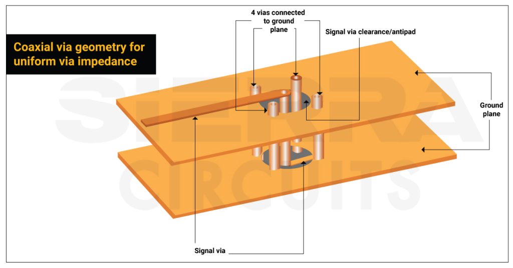
Incorporate coaxial via geometry
If a signal encounters an impedance discontinuity, it will generate jitters in PCBs and hamper the signal integrity.
You can reduce this effect by implementing a coaxial via structure.
Here, the via carrying the signal is placed at the center and is surrounded by 4 ground vias.
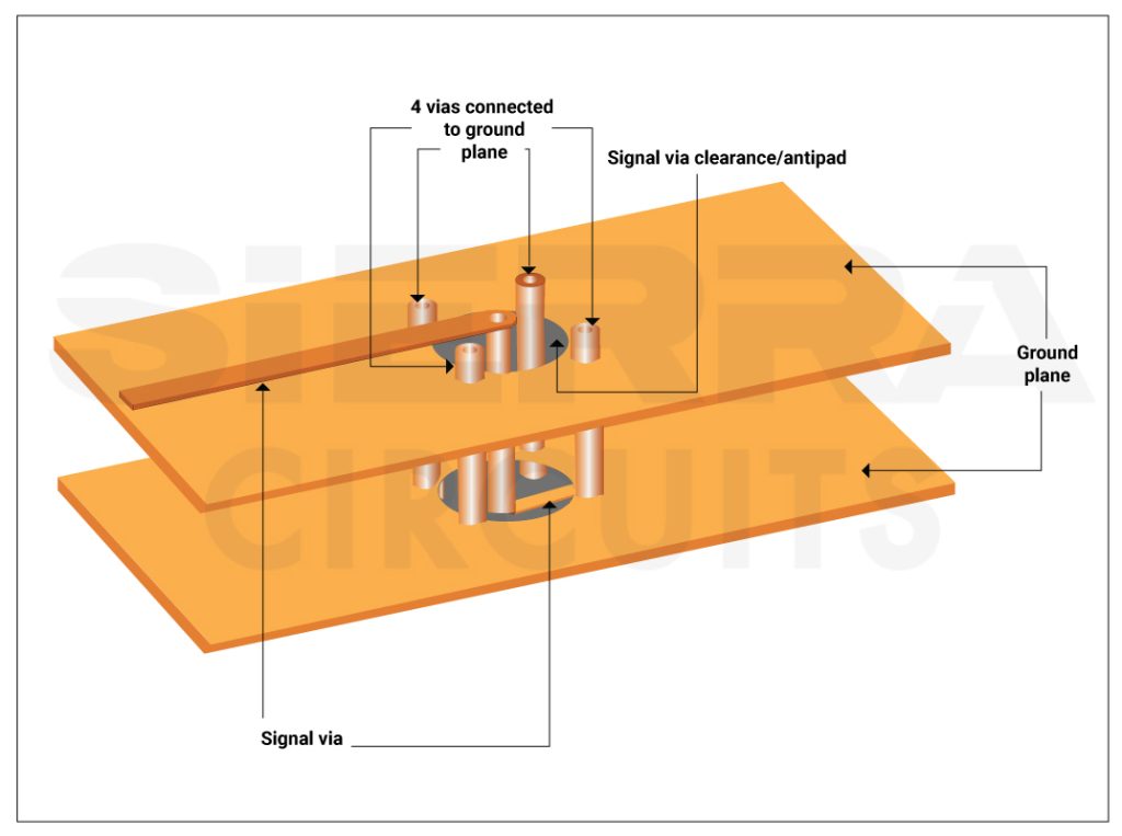
The ground vias pass through the antipad of the signal via. This induces homogeneous capacitance between each of the ground vias and the signal via.
The values of the capacitances depend on the via diameters, the dielectric constants, and the clearance between the signal and ground vias. This structure prevents a drastic shift in capacitance values in the via and ensures uniform impedance.
In addition, the ground vias form an inductance loop between the signal and ground vias and aid in establishing a proper return path.
To minimize via impedance discontinuity, you can opt for a coaxial via structure with a minimum of 2 and a maximum of 4 ground vias surrounding a signal via.
Keep the current return path as close as possible
Return current chooses the lowest inductance path. The signal has a tendency to select the path just below the signal line.
However, in high-speed data communications, multiple signals share the same starting and terminating point. Due to this, the return signal might not choose the dedicated ground path.
This factor leads to impedance discontinuity and disrupts signal transmission.
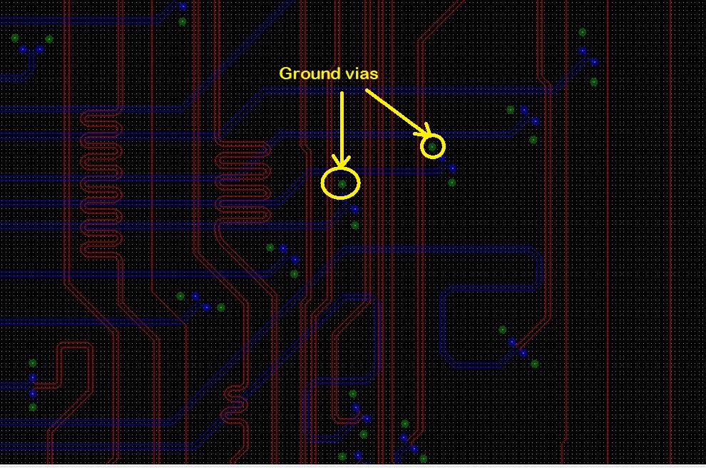
To avoid impedance discontinuity, have the ground via near the signal via. This creates a low inductance loop between the signal via and the ground via ensuring an effective return path. The current can bypass the inductance loop even if there is an impedance mismatch in the via. Hence, signal quality is maintained.
How to calculate via impedance quickly
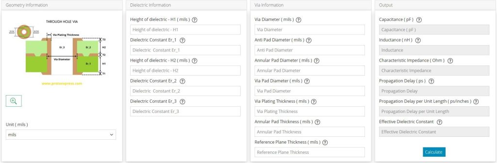
You can use Sierra Circuits’ Via Impedance Calculator to compute via impedance, capacitance, and inductance. This easy-to-access tool incorporates 2D numerical solutions of Maxwell’s equations to render accurate and consistent results.

Methods to identify via impedance discontinuity
TDR
TDR measurement is the conventional yet fruitful approach to determine impedance discontinuity in a via. This device feeds a pulse onto the selected via to measure the reflections. If the via has a uniform impedance and is properly terminated, there will be zero reflections, and the incident pulse will be absorbed in the far end by the termination.
On the contrary, if there are impedance variations, some incident signals will be reflected back to the source. TDR measures the propagation velocity of the received pulse and detects the location of impedance mismatch. This will be displayed in the waveform, using which the characteristic impedance is measured.
S-parameter analysis
S-parameters are also beneficial in analyzing reflection, loss, signal attenuation, and, therefore, impedance. For S-parameter analysis, you need to consider a via as a two-port network.
A 2-port DUT has four S-parameters. These can be calculated using the following equations:
S11 = b1/a1 = the input reflection coefficient
S12 = b1/a2 = the reverse transmission coefficient
S21 = b2/a1 = the forward transmission coefficient
S22 = b2/a2 = the reverse reflection coefficient
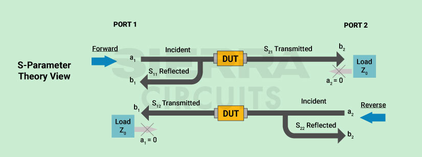
Where,
a1 = traveling wave incident on port 1
a2 = traveling wave incident on port 2
b1 = traveling wave reflected from port 1
b2 = traveling wave reflected from port 2
Via impedance is one of the critical aspects to consider if you’re working on high-speed applications, as it can directly impact the signal integrity. Implementing coaxial via structures and placing ground via close to the signal via can reduce the negative impacts of impedance discontinuity. If you have any queries regarding via impedance, let us know in the comments section. Our experts will be happy to help you.
About Poulomi Ghosh : Poulomi is a microwave engineer specializing in EMI, EMC, RF, and high-speed electronics. As a senior technical writer at Sierra Circuits, she creates advanced engineering articles and webinars for hardware engineers and PCB designers.