


Contents
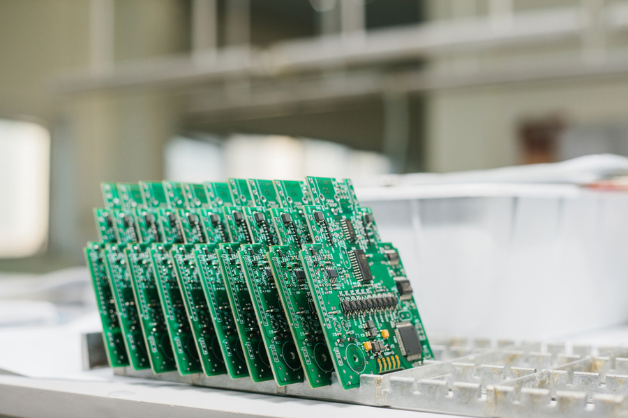
A quick-turn PCB holds a huge demand as it trims down the production time without compromising the quality of the board. If you need a quick and accurate idea of your final product performance, quickturn PCBs are the way forward.
This article will briefly give you an overview of what exactly quick turn PCB means, its benefits, and the factors that affect the turnaround time.
What is a quickturn PCB?
A quickturn circuit board is designed, fabricated, assembled, and tested in an extremely short duration. The turnaround time ranges from 24 hours to 7 days based on the design complexity.
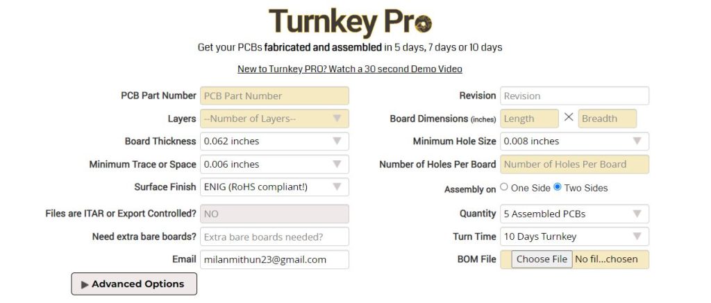
Use our Turnkey Pro quote engine to get an instant quick turn PCB quote

Benefits of Quickturn PCB orders
There are several reasons why quick-turn PCB prototyping is preferred.
- Facilitates faster testing of design ideas or components.
- Provides DFM assistance to reduce overall project costs and time-to-market.
- Determines product efficacy before investing in large-scale production.
- Supports the production of small quantities of prototype boards required for design and validation purposes.
For step-by-step guidance on getting your first prototype fabricated, read how to get your first PCB manufactured .
Sierra Circuits’ typical turnaround time for quickturn PCBs
The turnaround time (TAT) can vary depending on many aspects such as compliance with DFM/DFT, design files, and components availability.
| PCB type | Layers | TAT without assembly (in days) | TAT with assembly (in days) |
|---|---|---|---|
| Standard rigid | 1 to 6 | 1 | 2 |
| Standard rigid | 8 to 12 | 3 | 4 |
| Rigid-flex | 1 to 12 | 5 to 7 | 6 to 8 |
| Flex | 1 to 10 | 3 to 5 | 4 to 6 |
Please note that these TATs are applicable only for single lamination cycle boards.

Design for Manufacturing Handbook
11 Chapters - 96 Pages - 90 Minute ReadWhat's Inside:
- Annular rings: avoid drill breakouts
- Vias: optimize your design
- Trace width and space: follow the best practices
- Solder mask and silkscreen: get the must-knows
Download Now
Factors that affect the turnaround time of a prototype
Getting a quickturn PCB prototype is not science fiction. There are a few facts on PCB manufacturing that you simply need to acknowledge before you begin working on your design. Here’s what Amit Bahl has to say about the parameters that impact the turnaround time of a PCB.
Circuit board design and test procedures
Adhere to DFM and DFT guidelines to achieve superior quality boards. Verify component availability before using it in your prototype PCB design and work out the best layout strategies for a compact design. Providing clear test requirements and establishing a clear test protocol in advance is key for a rapid turnaround time.
Lamination cycles
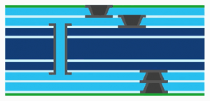
An HDI board that incorporates different types of via structures will need sequential lamination cycles. Every time you laminate a board, it is like building another multilayer board. It adds to the cost of the PCB. The lead time for quickturn advanced technology boards with multiple laminations will be more compared to that of standard technology boards.
The time required for a lamination cycle depends on the number of layers in the stack-up and the type of material chosen. On average, each extra lamination cycle usually adds 4-5 days to the process. This also includes the time taken for any type of drilling, plating, or filling. Apart from the time taken for lamination, one needs to consider an additional day to process the outer layers.
For example, the image above portrays the presence of a buried via (core) along with both stacked and staggered microvias. Such a board would have a 2+N+2 stack-up. The total number of lamination cycles required is three. The TAT for such a board would usually be 10-11 days.
Via-in-pad plated over
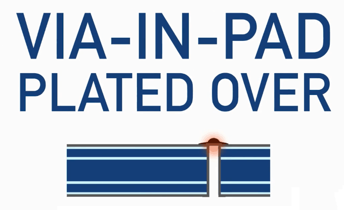
Amit says, “If you have a surface mount footprint with vias in the pad, it can cause the solder to wick into the hole. Sometimes this process may be required to keep heat out from under the component, or as a means of saving space. While via-in-pads have become very common, be aware that they can add at least a day to the cycle time.”
Fabrication drawing specifications
A fab drawing specifies important board manufacturing information like critical mechanical dimensions, IPC class, materials, layer stack-up, via drill chart, and plating thickness. It provides controlled impedance requirements and other tolerances.
You need to be cognizant of the manufacturer’s capabilities to bridge the gap between design vs DFM. For instance, be aware of the minimum trace width and space that can be accommodated in the manufacturing process to avoid design rework time delays. Always mention if your prototype needs to follow IPC class 2 or class 3 manufacturing standards.
Layer stack-ups must be carried out keeping in mind the availability of the materials and their cost. Few materials that are not commonly used may have a large lead time thereby increasing the turn-around time. Verify the controlled impedance table in the drawing. Ensure that it correctly identifies the target impedances and specific trace widths/spaces to be controlled. This will prevent delays due to information mismatch.
Surface finish
Another time-consuming process step is the surface finish. HASL and ENIG are the most commonly used coatings. On average, HASL takes around 15-20 minutes while ENIG takes around 90-120 minutes.
If your board requires two types of gold finishes — ENIG for surface mounts and hard gold for edge connectors—you are adding twice the time to the plating process. Each finish must be plated separately, and go through the complete process twice.
Assembly drawings and notes
Assembly drawings include information related to part lists, shapes, top and bottom views of the board, identification labels, and assembly-specific notes. Assembly drawings along with fab notes help in the inspection of the circuit board. Consider the following points to avoid delays during the board assembly process.
- Follow all the DFA rules. Confirm that there is no component footprint mismatch.
- Submit a complete BOM including the Manufacturers’ Part Numbers (MPNs) and descriptions.
- If you are supplying parts, follow kitting guidelines.
- Ensure that the silkscreen markings are legible. Markings need to clearly display all information necessary for assembling, testing, and troubleshooting of the circuit board. It must definitely include component reference designations and polarity indicators.

PCB Design for Assembly Handbook
6 Chapters - 50 Pages - 70 Minute ReadWhat's Inside:
- Recommended layout for components
- Common PCB assembly defects
- Factors that impact the cost of the PCB assembly, including:
- Component packages
- Board assembly volumes
Download Now
Choosing the right quickturn fabrication partner in the USA
Never rush the process of finding a good CM and ensure that you don’t compromise on quality over cost. Partnering with a certified CM who can offer turnkey PCBs has many benefits like reduced TAT and quality assurance. They will have a workforce who can provide a standard product using the latest technologies within the stipulated time.
Other factors that need to be considered are:
- Location: Location is a critical factor when it comes to prototyping efforts. Opting for a local CM can be an advantage in quickturn services. Naturally, the further away the fabrication partner is, the longer delivery will take. For turnkey projects, consider switching to onshore manufacturers who have a strong supply chain and established supplier contact base. By choosing a U.S.-based fabrication partner, your potential turnaround time immediately becomes much quicker.
- Product lead time: The sooner the fab-house produces your prototype, the sooner you can finalize your design for large-scale production.
- Certifications: Make sure that the manufacturer’s operations are in conformance with global quality standards like IPC, ISO, UL, RoHS free and possess certifications. Visit our certifications and registrations page to know the standards we conform to.
- Consistency: Your CM should repeatedly deliver quality boards, both at small-scale and large-scale.
- Communication and support: Regular communication with your CM is vital. Your manufacturer should be able to offer in-depth support that you need in each stage of prototyping. Your concerns should be immediately addressed.
These are just a few things to consider before production begins. Having this information ahead of time will give you a realistic schedule. See case study: quickturn PCB for Bluetooth application where one of our esteemed clients talks about our ability to support their design requirements.
Why should you choose Sierra Circuits as your preferred partner?
Sierra Circuits can be your perfect partner for quickturn PCBs. We cater to IoT, military, medical, aerospace, consumer electronics, and OEMs. Our strengths include:
- State-of-the-art facilities with advanced machinery and equipment such as LDI, laser drills, and solder mask spray coating machines.
- More than 100 man years of experience in board design and manufacturing
- Engineering team that validates and supports your design 24/7
- Certified with all the necessary industry standards
- Offer advanced design tools to expedite your design process.
Quickturn PCB fabrication is the most efficient and cost-effective way to manufacture your prototypes. A skilled manufacturing partner will offer collaborative efforts so that your final product is the best. We at Sierra Circuits understand your design goals and execute your ideas rapidly giving you a competitive advantage. Let us know in the comments section if you require any design-related assistance. Our experts will be happy to help you. Also, visit the design services page to know more about our capabilities.

About Amit Bahl : Amit Bahl, widely recognized as the PCB Guy, earned his Bachelor of Science in Engineering from UCLA. He is currently the Chief Revenue Officer at Sierra Circuits, where he continues to lead efforts to simplify the PCB design journey and support designers and engineers in creating high-quality boards.


Start the discussion at sierraconnect.protoexpress.com