


Contents

On-demand webinar
How Good is My Shield? An Introduction to Transfer Impedance and Shielding Effectiveness
by Karen Burnham
At 28-56-112 Gbps, a high-speed PCB connector is much more than a mechanical interface; it is an extension of the signal path. As data rates rise, even small electrical discontinuities become harder to ignore. A poorly designed connector interface, an interrupted reference plane, or a slight change in trace geometry can introduce reflections, insertion loss, and crosstalk.
The challenge is that the connector cannot be designed independently. The launch geometry, transmission lines, and return paths must work together as one high-speed channel.
In this article, we examine the key signal integrity challenges at high-speed connector interfaces and provide practical design techniques for controlling signal losses and degradation.
Watch the full webinar here: High-speed success at 28-56-112 Gbps with connector-PCB integration.
Highlights:
When designing a connector interface:
- Maintain consistent trace width
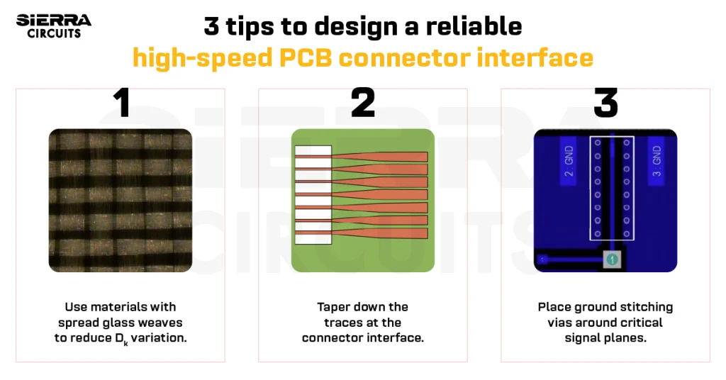
- Use gradual tapers for unavoidable neck-downs
- Place stitching vias close to signal transitions
- Match connector impedance with the transmission line
Why do connectors matter in high-speed PCB designs?
Connectors are generally a part of the high-speed signal path and can directly affect impedance, reflections, insertion loss, and return loss.
At higher data rates, the connector, vias, and reference planes work together as a tightly coupled electromagnetic system. As a result, design decisions that may be acceptable at lower speeds can introduce signal integrity problems at higher data rates.
Here’s why high-speed connectors require a fundamentally different approach to PCB design:
1. The connector is part of the transmission line, not a discrete component
At lower speeds, connectors could often be treated as discrete interconnects with relatively small electrical effects. At 28-112 Gbps and in RF applications, that assumption no longer works.
It becomes an extension of the transmission line, and its physical construction directly affects the electrical performance of the channel.
Pin geometry and arrangement can influence:
- Impedance profile
- Insertion loss
- Return loss
As a result, the connector cannot simply be selected and attached to the PCB after the routing is complete. Its electrical model, typically S-parameters, should be included in channel analysis before the layout is finalized.
2. The connector-to-PCB interface becomes a critical discontinuity
In conventional circuit board design, connectors were often treated as discrete components with minimal electromagnetic impact. In reality, the high-speed PCB connector launch region might often cause the worst discontinuity in the entire channel.
The electrical behavior of this transition depends on several physical features, including:
- Pad geometry
- Antipad size and shape
- Via placement around the connector
- Reference plane transitions
A poorly designed launch creates reflections that can degrade the channel’s insertion and return loss. At high data rates, those reflections can contribute to eye closure, jitter, and higher bit error rates.
3. Via stubs can become resonant structures
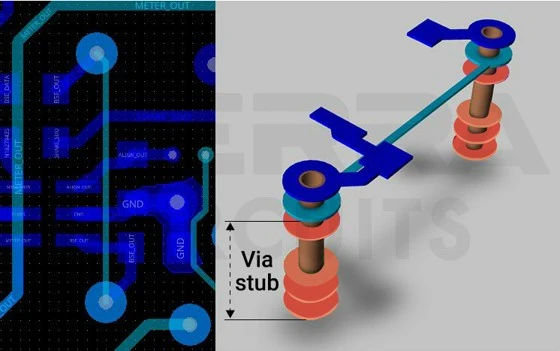
At high frequencies, a via is no longer just a convenient vertical connection between board layers. Its geometry introduces parasitic effects, which can alter the impedance of the signal path.
Unused via stubs are particularly problematic because their electrical length can become significant at high frequencies. Depending on the stub length and signal frequency, the stub can behave as a resonant structure and produce frequency-dependent impedance discontinuities.
These effects can appear as:
- Reflections
- Increased insertion loss
- Return-loss degradation
- Resonant notches in the channel response
For this reason, high-speed connector transitions often require careful via design, including optimized pad and antipad geometry, short stubs, backdrilling, or alternative via structures where appropriate.
4. Return path discontinuities can impact signal integrity
High-speed current does not travel only along the signal trace; it also requires a low-impedance return path. Any discontinuity in that path can alter the electromagnetic field distribution and increase the effective inductance of the current loop.
Common problems include:
- Plane splits or gaps
- Reference-plane transitions
- Poorly placed return vias
- Inadequate ground stitching
- Cavity resonances
These discontinuities can increase crosstalk, degrade signal quality, and contribute to electromagnetic interference. At high data rates, even a relatively small disruption near a connector launch or layer transition can affect the channel.
During an interview, Dilip Kumar, Senior Design Manager at Sierra Circuits, explained, “Before designing a high-speed connector interface, review the connector datasheet carefully. Verify its impedance, pin arrangement, differential-pair configuration, and operating frequency, and then optimize the PCB launch to match these characteristics. This minimizes impedance discontinuities and reflections at the connector-to-PCB transition.”
For more guidelines, download the Connector Design Guide.
Connector Design Guide
5 Chapters - 32 Pages - 50 Minute ReadWhat's Inside:
- Basics
- Terminology
- Selection and layout rules
- Testing
- Application-specific PCB connectors
Download Now
What are the challenges in designing high-speed connector interfaces?
Designing connector interfaces presents 3 major challenges: maintaining uniform impedance across the signal path, managing crosstalk near the connector, and minimizing insertion loss. At 28, 56, and 112 Gbps, even small discontinuities in trace geometry, reference planes, or connector transitions can affect signal integrity.
During the webinar, we asked engineers about their biggest challenges in designing PCB-to-connector interfaces.
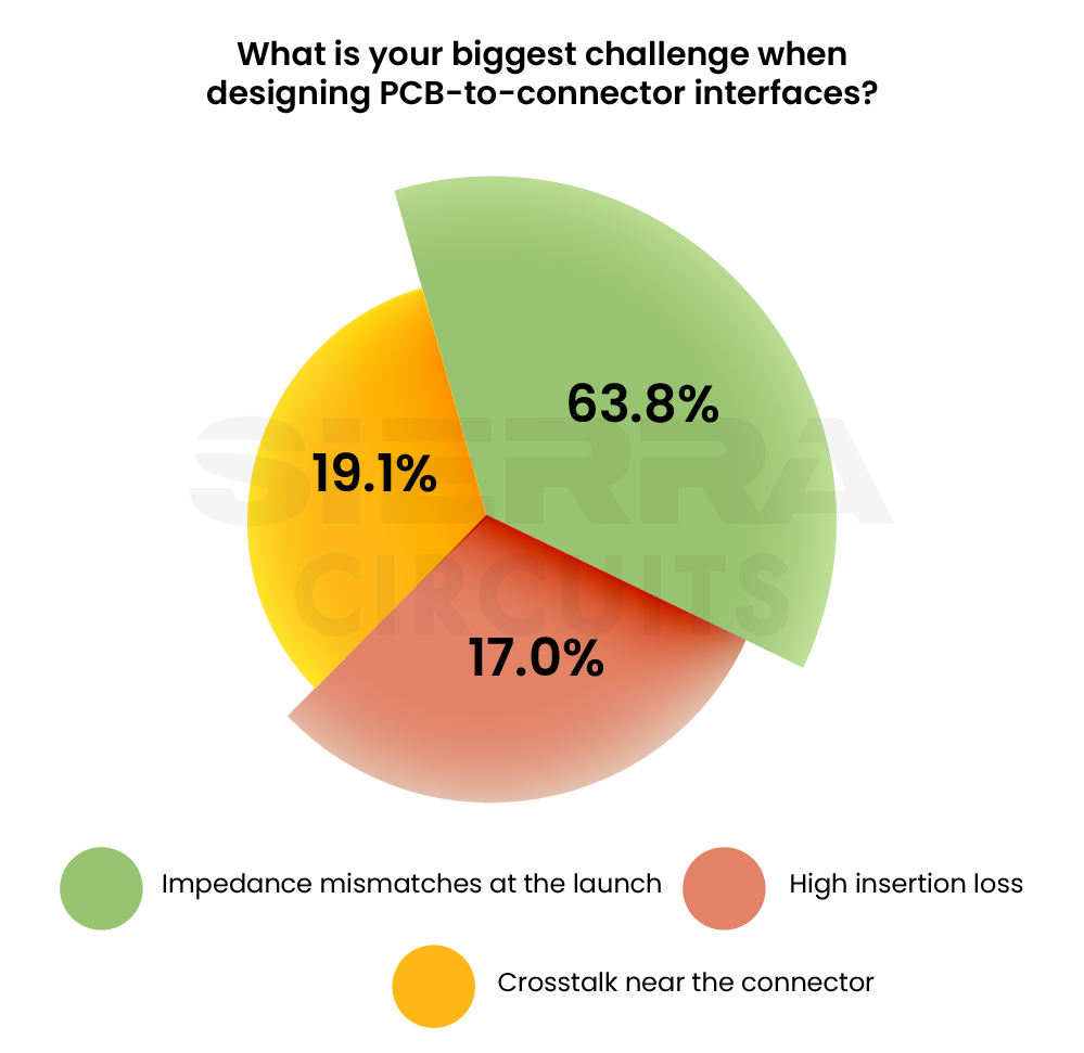
Here’s the poll result:
- 63.8% struggle with impedance mismatches at launch.
- 19.1% encounter crosstalk near the connector.
- 17.0% find challenges with high insertion loss.
In this section, you’ll learn practical solutions to address these three significant challenges.
1. Ensuring uniform impedance across connector interfaces
At 28, 56, and 112 Gbps, impedance is no longer simply a value to achieve during PCB design; it must remain consistent across the entire signal path. Any abrupt change in trace geometry, dielectric environment, reference plane, or transition structure can create an impedance discontinuity. These impedance discontinuities generate reflections that degrade signal integrity and reduce system margin.
Here are the techniques to minimize impedance discontinuities:
1.1 Maintain consistent trace width
A change in trace width changes the local impedance and can introduce reflections into the channel. The goal is not simply to achieve the target impedance at one point, but to maintain it as consistently as possible along the entire channel.
Any deviation in width alters the impedance locally. Even small variations can:
- Create impedance discontinuities
- Introduce reflections
- Distort the transmitted signal
At high data rates, these effects accumulate and significantly impact eye diagrams. To avoid these issues:
- Keep trace width consistent throughout the routing path.
- Avoid unnecessary width changes or abrupt neck-downs.
- Calculate the required trace geometry from the actual PCB stack-up using an impedance calculator or field solver.
- Account for changes in dielectric thickness and reference-plane configuration when routing across different layers.
1.2 Use gradual tapers for unavoidable neck-downs
In areas such as BGA breakouts, connector launches, and dense routing regions, maintaining the nominal trace width may not always be practical. A trace may need to be narrowed to escape a fine-pitch component or transitioned to a different geometry.
An abrupt width change creates an impedance step and can produce reflections. A gradual taper spreads this transition over a longer distance, reducing the severity of the discontinuity.
Here are the practical tapering guidelines:
- Use a gradual transition rather than a sudden step.
- Make the taper long enough to avoid an abrupt electrical transition; the required length depends on the stack-up and signal bandwidth.
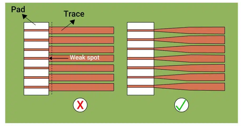
- Maintain symmetry when tapering differential pairs.
- Verify critical transitions with a 2D/3D field solver or channel simulation when margin is limited.
1.3 Keep high-speed signals away from strong aggressors
Controlled impedance alone does not guarantee signal integrity. High-speed traces can pick up unwanted energy through capacitive and inductive coupling from nearby switching structures.
Potential aggressors include:
- Switching-regulator nodes and high-di/dt current loops
- Fast clock and data traces
- High-current power paths
- Connectors carrying noisy signals
- Dense via fields associated with power or switching circuitry
To reduce unwanted coupling:
- Maintain adequate spacing from known aggressors.
- Route high-speed signals over a continuous reference plane.
- Keep high-speed routing away from switching-node copper and high-current loops.
- Use ground shielding or stitching vias where they provide a clear electromagnetic benefit.
- Avoid long parallel trace routing; instead, use orthogonal trace routing on adjacent layers.
For more, see 10 best high-speed PCB routing practices.
1.4 Have constant geometry for differential pairs
Differential signaling depends on the controlled relationship between the two conductors. Differential impedance is influenced by trace width, trace-to-trace spacing, dielectric thickness, and the reference-plane structure.
Changes in width, spacing, routing environment, or reference plane can disturb that balance and cause mode conversion, where some differential-mode energy is converted into common-mode energy.
To maintain differential integrity:
- Keep trace width and pair spacing as consistent as practical.
- Route the pair together and avoid unnecessary separation.
- Maintain the same reference-plane structure beneath both traces.
- Avoid routing one trace through a different electromagnetic environment than the other.
- Use symmetric transitions through vias, connector launches, and layer changes whenever possible.
1.5 Match the connector impedance with the transmission line
The connector-to-PCB interface is one of the most critical impedance transition points in the channel. If it does not match the PCB transmission line:
- Signal reflections occur at the interface
- Return loss increases
- Overall channel performance degrades
To overcome these challenges:
- Select connectors with impedance matching your PCB (typically 85 Ω or 100 Ω differential).
- Optimize launch geometry (pad size, antipads, via structure).
- Use vendor-provided models (S-parameters) for validation.
1.6 Optimize meander spacing during length matching
Length matching is often necessary to control skew between signals, but tightly packed serpentine routing can introduce another form of coupling.
When adjacent segments of a meander run too close together, they can couple electromagnetically. This can alter the effective propagation delay and create localized impedance variations. The result is that a trace that is geometrically length-matched may not be electrically equivalent to a straight trace of the same length.
To minimize meander-related coupling:
- Provide sufficient spacing between adjacent segments.
- Avoid unnecessarily tight, repeated zig-zag patterns.
- Use smoother and more widely spaced tuning structures where board space permits.
- Keep coupled segments as short as practical.
- Consider phase tuning or other length-matching techniques when appropriate.
A useful starting point is to keep adjacent meander segments separated by several trace widths, but the exact spacing should be determined from the stackup, geometry, and required coupling performance.

2. Managing crosstalk in high-speed PCB connectors
At high speeds, signals travel as electromagnetic fields, not just current through copper traces. Crosstalk occurs when electromagnetic energy from one signal trace couples into a nearby trace or structure. It becomes more significant when return currents and electric or magnetic fields interact with adjacent conductors, increasing unwanted capacitive and inductive coupling.
The following practices help manage crosstalk in high-frequency designs with connectors:
2.1 Avoid plane splits under high-speed signals
- Route critical high-speed signals over continuous ground or reference planes.
- Avoid crossing plane splits, slots, voids, or large anti-pad regions.
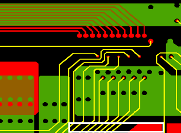
- Keep differential pairs over the same continuous reference structure.
- During layout review, examine the signal layer and its adjacent reference plane together, rather than reviewing the signal routing in isolation.
For very high-speed interfaces, even a relatively small reference-plane discontinuity can become significant because the relevant frequency content extends well beyond the nominal data rate.
2.2 Incorporate stitching vias close to signal transitions
When a high-speed signal changes layers through a via, its return current may also need to transition between reference planes. Without a nearby return path, the current can be forced to travel through a longer route, increasing loop inductance.
Ground-stitching vias provide a low-inductance connection between reference planes, allowing the return current to transition more directly.
Place stitching vias:
- Close to signal-via transitions
- Near connector launches
- Around reference-plane boundaries
- Near the edges of high-speed regions where field containment is important
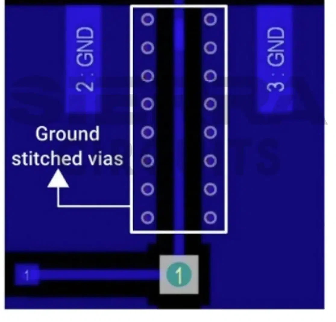
A commonly used starting point for stitching-via spacing is λ/20 to λ/10 at the highest significant frequency of interest, but this should be treated as a design guideline rather than a universal rule. The actual spacing should account for the signal’s frequency content, stack-up, via geometry, and electromagnetic behavior.
The objective is to keep the return path electrically short and prevent the return current from spreading into a large loop area.
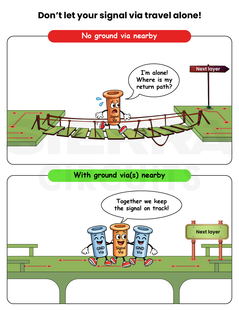
2.3 Maintain appropriate via pairing
When a signal via transitions between layers, provide a nearby ground via or ground-via fence so the return current has a low-inductance path between the corresponding reference planes.
A practical layout approach is to:
- Keep the signal-to-ground-via spacing as small as practical.
- Place one or more ground vias close to the signal via.
- Maintain a consistent via arrangement across similar high-speed transitions.
- Use multiple ground vias when required to reduce inductance and improve field containment. The exact spacing should be determined by the stack-up, via dimensions, signal bandwidth, and connector geometry.
For differential signals, maintain a symmetrical via arrangement wherever possible to minimize common-mode conversion and preserve differential-mode behavior.
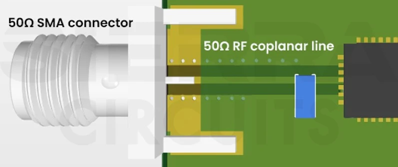
2.4 Use coplanar waveguide structures
A grounded coplanar waveguide (GCPW) places ground copper on the same PCB layer alongside the signal trace, while also using a reference plane beneath the trace.
This structure can provide:
- Better electromagnetic-field confinement
- Reduced coupling to neighboring structures
- Improved impedance consistency
- A well-defined return-current environment
- Reduced radiation from the transmission line
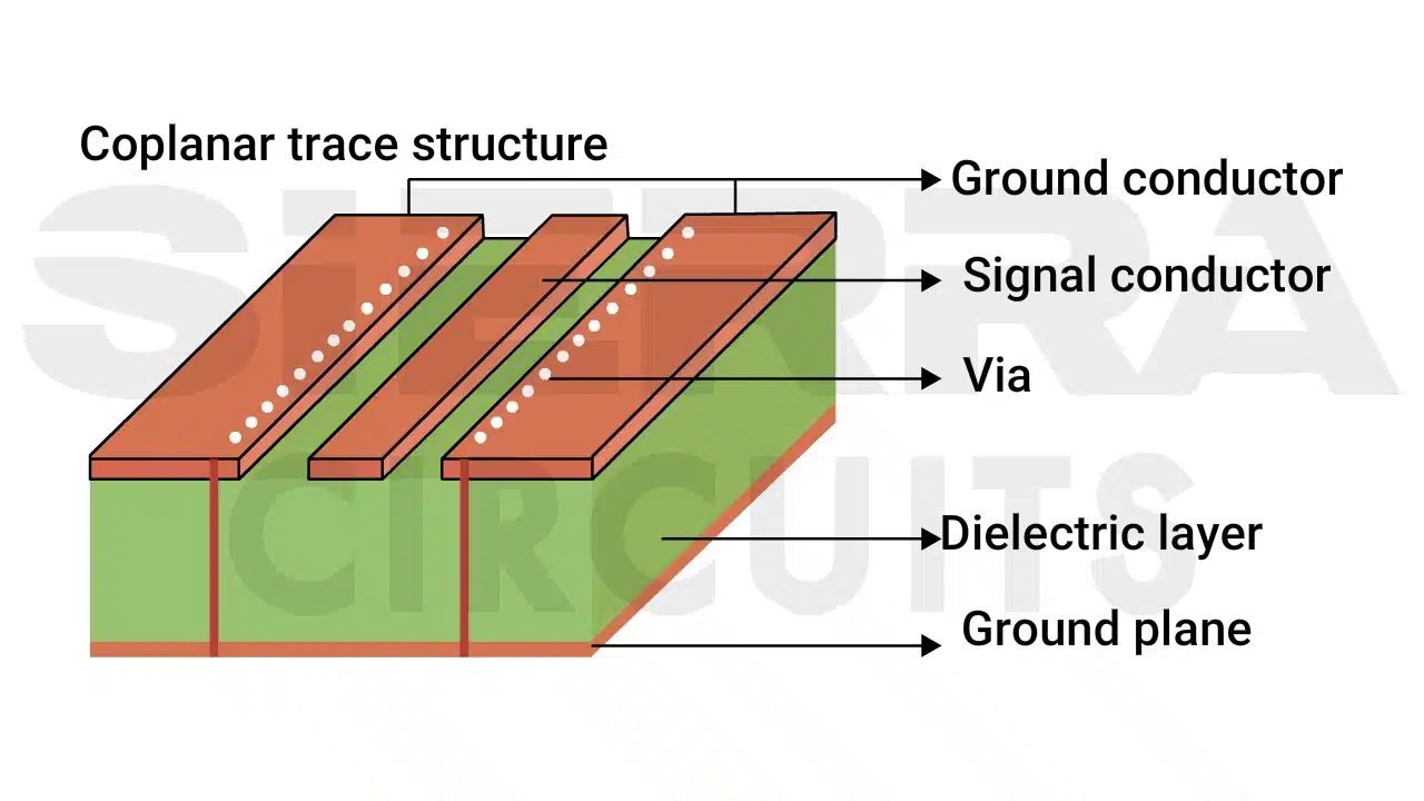
Ground vias can be placed along the coplanar ground regions to connect the top-layer ground to the underlying reference plane. However, the spacing between the signal trace and adjacent ground copper must be carefully controlled because it directly affects the transmission-line impedance. The geometry should therefore be modeled using the actual stack-up and material properties rather than selected arbitrarily.
2.5 Minimize return path interruptions during routing
Return current needs a continuous, low-impedance path.
During routing, avoid:
- Large via anti-pads
- Plane voids
- Connector cutouts
- Plane gaps and splits
- Unnecessary layer transitions
- Changes between reference planes
- Areas where the reference plane changes from ground to power
- High-density BGA escape regions
3. Reducing insertion loss
If you do not select an appropriate material, even a well-designed connector footprint can encounter signal loss.
Here are 4 key material considerations to minimize insertion loss at the connector-to-board interface:
3.1 Choose a material with a low dielectric constant (<4)
The dielectric constant (Dk) determines how electromagnetic fields propagate through the circuit board.
- Lower Dk means higher signal speed and lower capacitance
- Directly affects trace impedance and connector launch geometry
- A Dk variation of even ±0.1 can shift impedance by several ohms
- This becomes critical in tight differential impedance budgets (e.g., 85 Ω /100 Ω)
- Non-uniform Dk across the board leads to inconsistent connector performance
- Have a tight tolerance (±0.05 to ±0.1) to ensure consistent impedance.
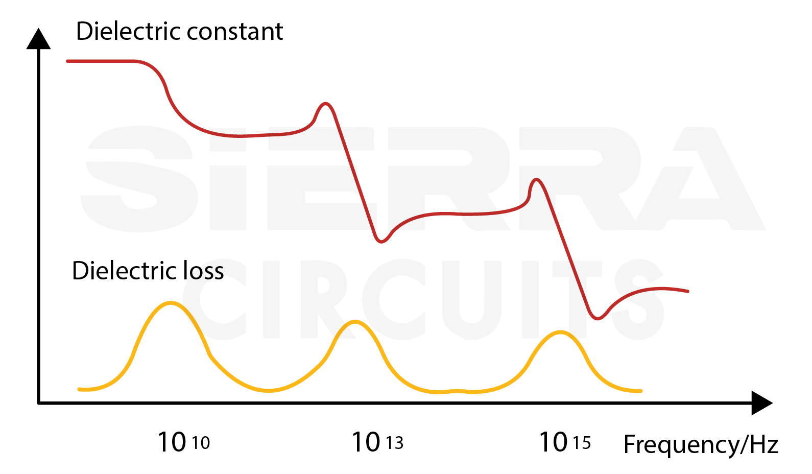
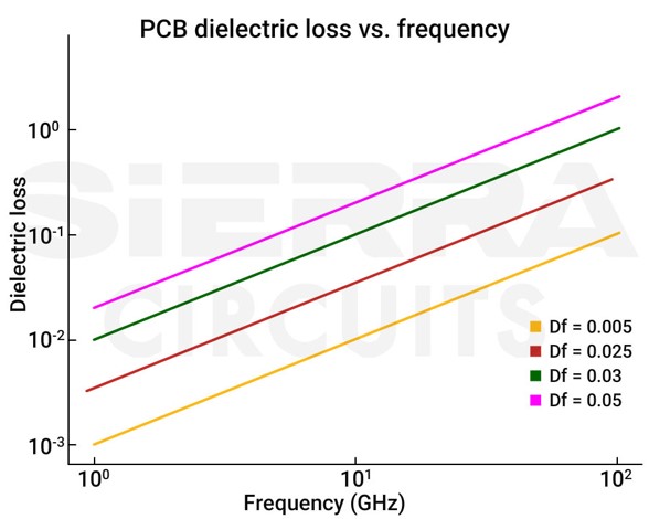
3.2 Pick a laminate with a low dissipation factor (<0.005)
Dissipation factor (Df) represents how much signal energy is lost as heat.
- Higher Df means more dielectric loss and reduced signal amplitude
- It strongly impacts insertion loss and eye diagram closure
It hurts the most in long channels with connectors (backplanes, mezzanine connectors) and at high frequencies (>10 GHz, typical in SerDes links).
Incorporate materials with Df <0.005 to reduce dielectric loss for long channels.
3.3 Select a low-profile or rolled-annealed copper
At high frequencies, current tends to flow near the conductor surface due to the skin effect.
- Rough copper increases the effective path length, increasing loss
- It leads to higher insertion loss and phase distortion
- Roughness becomes critical above ~5-10 GHz
- Connector launches are especially sensitive because they already introduce discontinuities
At 10 GHz, an increase of 1 μm in roughness results in an additional loss of 0.3 dB/m. Use low-profile (LP), very-low-profile (VLP), or rolled-annealed (RA) copper.
| Foil type | Surface roughness (Rz) | Insertion loss |
|---|---|---|
| HVLP / ULP | Lowest (< 1.5 μm) | Lowest |
| VLP | Low (≈ 2.0 μm) | Low |
| RTF | Moderate (3.0–5.0 μm) | High |
| Standard foil | Highest (> 5.0 μm) | Highest |
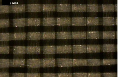
3.4 Opt for laminates with spread glass weave
At first glance, PCB dielectric material looks uniform, but internally, it’s a woven structure of glass fibers embedded in resin. The key issue is that glass and resin have different dielectric constants:
- Glass fiber: higher Dk (~5-6)
- Resin: lower Dk (~2-3)
This creates a non-uniform dielectric environment across the PCB. When a high-speed signal propagates along a trace, the effective Dk it sees depends on whether it is traveling over glass bundles or resin-rich areas.
In high-speed designs, especially with differential pairs, the two traces are routed very close together. Ideally, both traces should experience identical electrical conditions. But due to the glass weave pattern:
- One trace may run over glass-rich regions (higher Dk → slower signal propagation)
- The other may run over resin-rich regions (lower Dk → faster propagation)
This creates a velocity mismatch, which leads to differential skew. This problem becomes much more serious near connectors.
Connectors assume that:
- Differential signals arrive simultaneously
- The fields remain balanced and symmetric
But with skew:
- One signal enters the connector pin before the other
- The differential signal is no longer perfectly balanced
Use spread glass materials (e.g., 1067, 1086). These distribute glass fibers more evenly, reducing Dk variation.
Not sure whether your high-speed PCB design meets signal integrity requirements? Schedule a design review with our engineers to validate materials, impedance, and stack-up.

What stack-up mistakes can impact high-speed PCB designs?
An incorrect dielectric thickness, missing reference plane, unbalanced construction, or unsuitable copper weight can undermine impedance control before a single trace is routed.
Without a properly designed stack-up, it is difficult to establish consistent electromagnetic environments for high-speed signals. Before optimizing a high-speed PCB connector launch or tuning a differential pair, make sure the stack-up is both electrically and physically achievable.
The following 5 scenarios show how small stack-up decisions can create significant fabrication and signal-integrity challenges and how they can be corrected during the design stage.
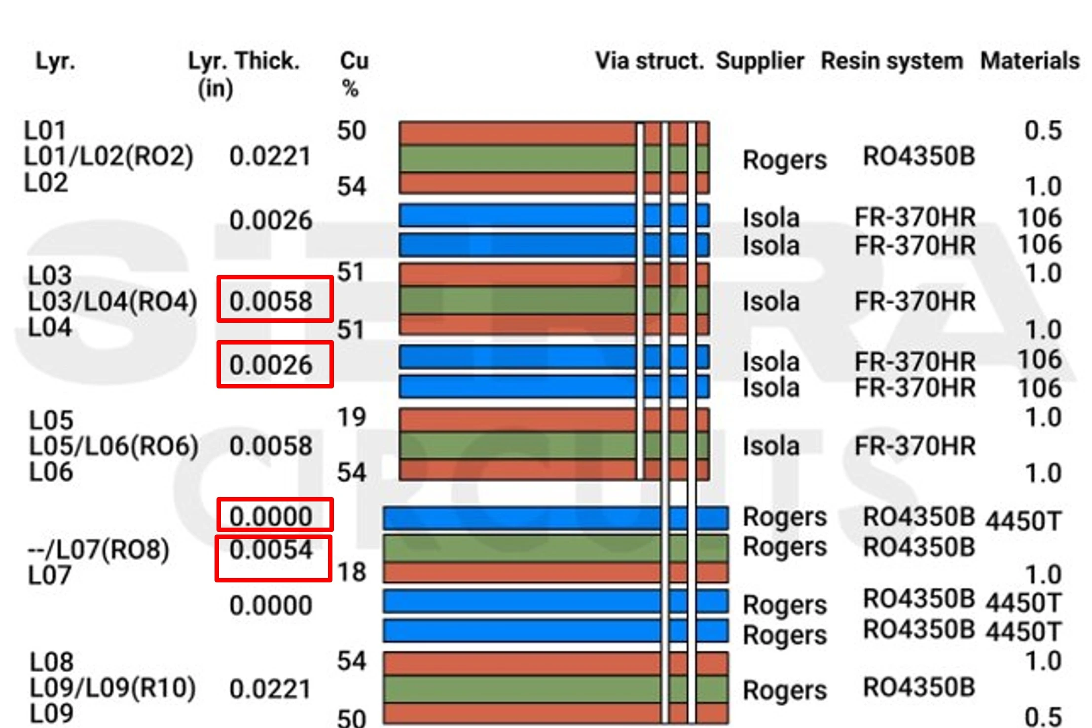
1. Unbalanced stack-up
An asymmetric stack-up leads to:
- Board warpage during fabrication
- Uneven mechanical stress
- Reliability issues over temperature cycles
Balanced stack-ups ensure uniform copper and dielectric distribution across the center plane.
2. Missing reference planes
High-speed signals require a continuous return path. If a signal layer lacks an adjacent reference plane:
- The return current is disrupted
- EMI increases
- Impedance becomes unstable
3. Copper weight mismatch
Copper thickness directly impacts impedance. Undefined or inconsistent copper weights can:
- Shift impedance away from the target
- Affect current-carrying capability
- Create fabrication variability
4. Incorrect dielectric thickness
Designers may specify dielectric thicknesses that are unavailable from the manufacturer or do not meet fabrication constraints. This can lead to redesign cycles and production delays.
Using an incorrect dielectric thickness in impedance calculations can result in:
- Wrong trace widths
- Impedance mismatch in fabricated boards
5. Ignoring the solder mask surface finish
Solder mask and surface finish add to the total thickness. Ignoring them leads to:
- Incorrect impedance values
- Stack-up errors
How to design manufacturable stack-ups
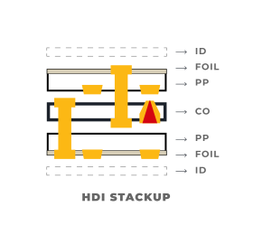
A manufacturable build-up should balance electrical performance, mechanical stability, and fabrication capabilities. Small changes in dielectric thickness, copper weight, or layer arrangement can affect signal integrity and board reliability.
Consider the following guidelines to create a stack-up that meets your design requirements while remaining practical to manufacture:
- Place signal layers next to solid reference planes to ensure clean return paths and controlled impedance.
- Maintain consistent dielectric thickness (<0.2 mm) to preserve return path continuity and impedance stability.
- Use symmetrical stack-ups. This technique prevents warpage and improves manufacturability.
- Choose appropriate copper weights, ~1 oz for signal layers and ~2 oz for power planes
- Define fabrication sequence clearly. Include the solder mask before the surface finish.
- Account for solder mask thickness, especially for the outer layer impedance.
- Specify complete stack-up details:
- Material type
- Dielectric thickness
- Copper weight
- Impedance targets
- Tolerances (typically ±10%)
The following real-world examples highlight common stack-up issues and how they can be corrected during the design stage to create a more reliable and fabrication-ready printed board.
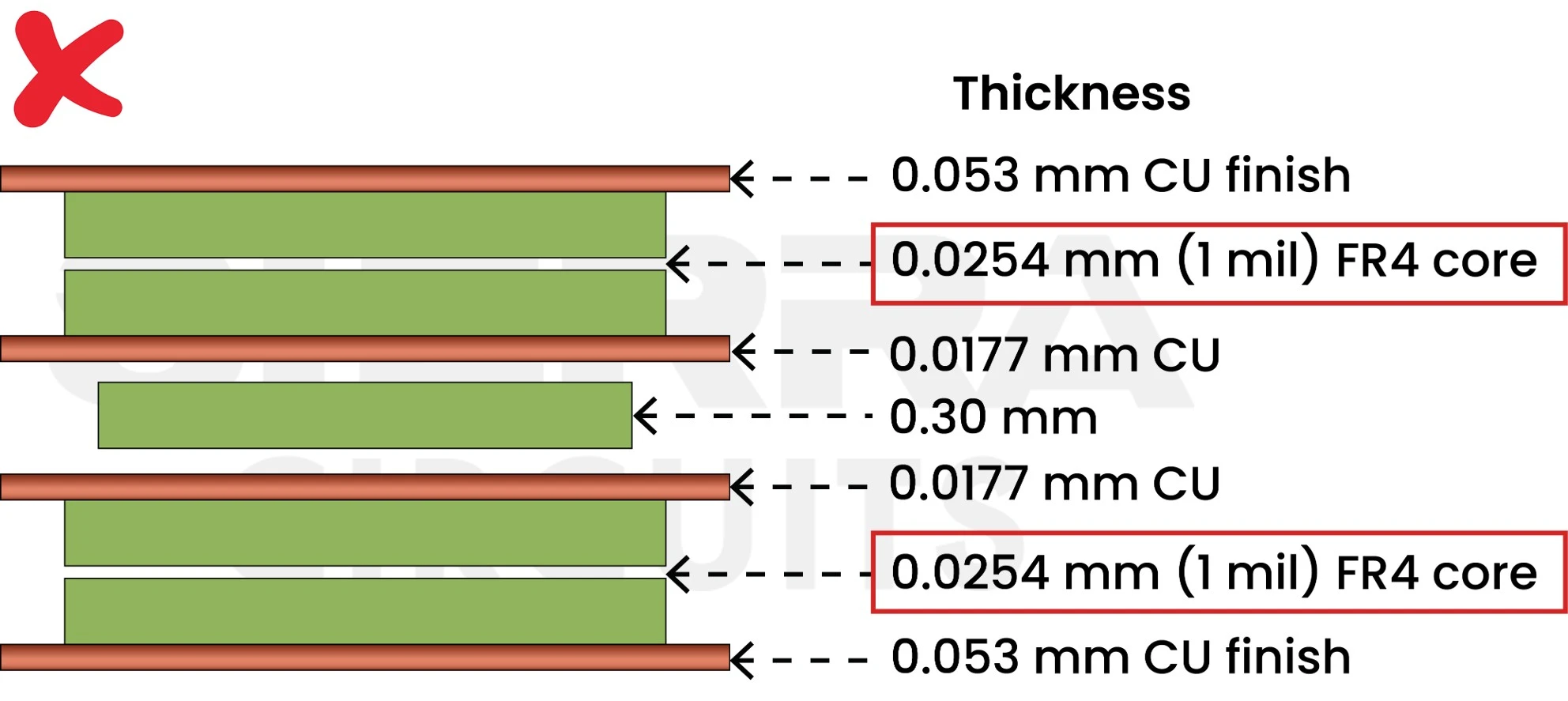
Case study 1: The 1-mil core that couldn’t be built
In this case, the original stack-up specified a 1 mil (0.0254 mm) FR4 core, which is not a standard or commercially available thickness.
Such unrealistic specifications create immediate fabrication challenges, as manufacturers cannot source or process such thin cores reliably. This would lead to delays or even build failure.
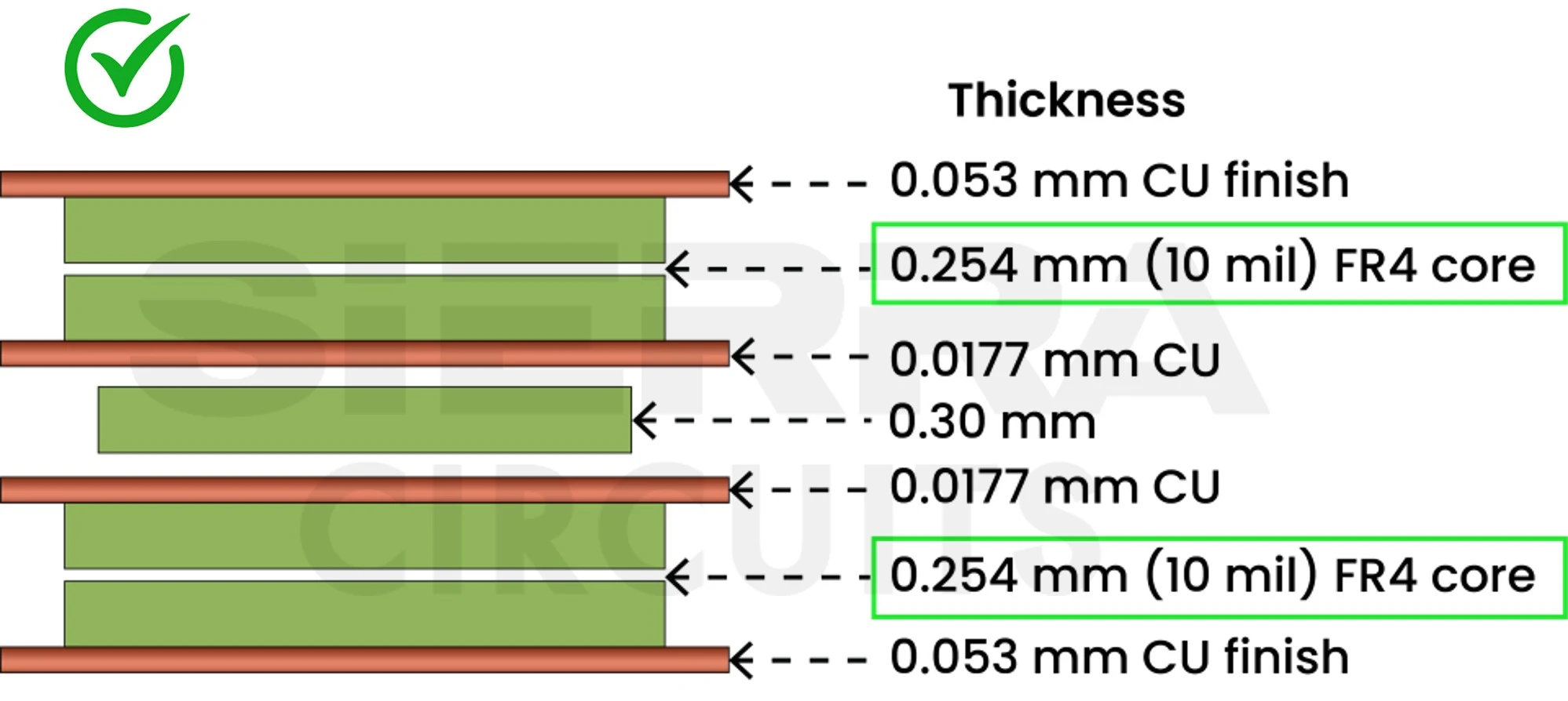
To resolve this issue, the core was replaced with a standard 10 mil (0.254 mm) FR4 core, which aligns with industry capabilities. This change ensured smooth fabrication, improved mechanical stability, and ultimately resulted in a manufacturable PCB without compromising performance.
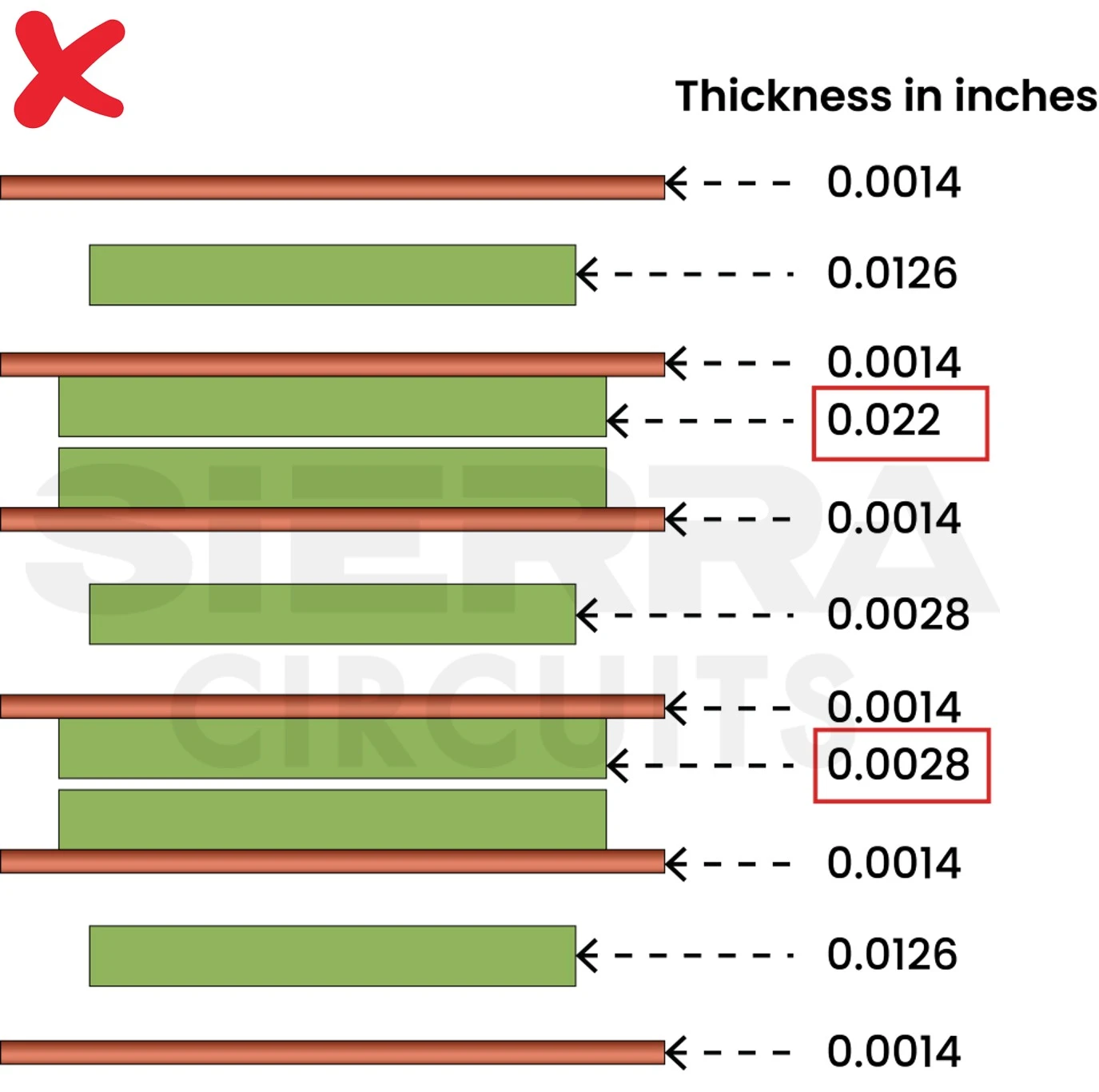
Case study 2: An asymmetric stack-up that might cause warpage
The build-up had an uneven dielectric thickness distribution. The layer structure was not mirrored across the center of the board. This asymmetry creates mechanical stresses during lamination and thermal cycling, leading to board warpage, layer misalignment, and potential reliability issues over time.
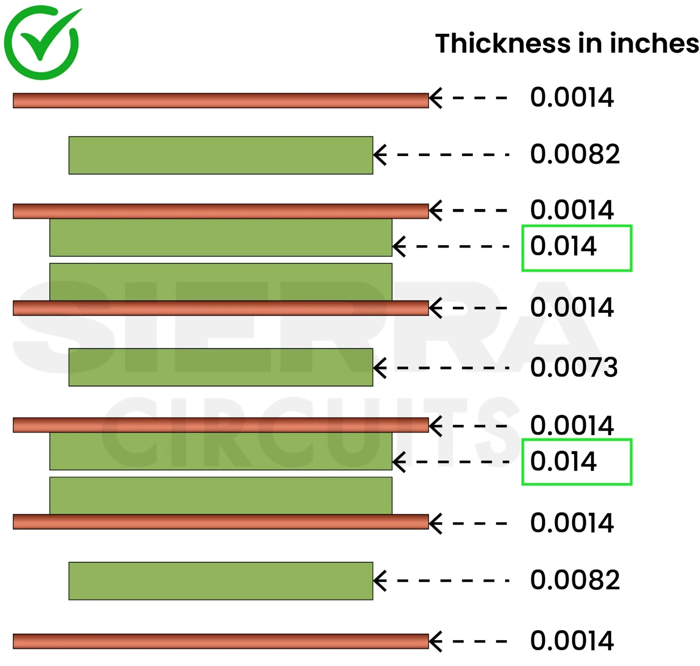
To fix this, our CAM engineer modified the dielectric thicknesses to form a symmetrical stack-up, ensuring equal dielectric thickness distribution above and below the centerline. This correction significantly reduced warpage and improved the board’s mechanical stability.
Need help resolving potential fabrication issues? Book a meeting with our experts, or call us at +1 (800) 763-7503.
What are the types of high-speed PCB connectors?
The three common types of high-speed connectors are board-to-board, backplane, and wire-to-board connectors. Each type serves a different application and presents unique signal integrity challenges based on channel length, connector geometry, and the transition between the connector and printed board.
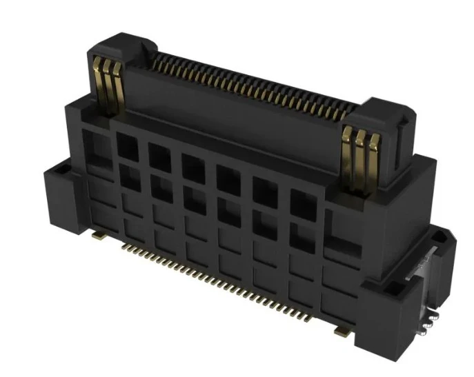
1. Board-to-board connectors
Board-to-board connectors are widely used in compact, modular electronic systems where multiple PCBs are stacked or placed side-by-side. These are commonly referred to as mezzanine connectors. They are designed to support:
- High pin density (hundreds to thousands of contacts)
- Differential signaling with tightly controlled impedance (typically 85Ω or 100Ω)
- Short channel lengths, which help reduce overall insertion loss
However, their compact form factor introduces several signal integrity challenges. As pitch decreases, crosstalk between adjacent differential pairs increases, and maintaining consistent impedance across all pins becomes more difficult.
Additionally, the connector launch region must be carefully tuned. Even slight misalignment between connector pads and PCB traces can introduce impedance discontinuities.
2. Backplane connectors
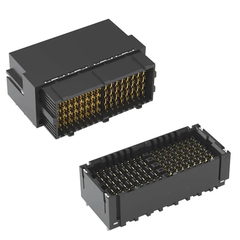
Backplane high-speed PCB connectors are used in high-performance systems such as telecom infrastructure, data centers, and servers. They connect multiple line cards to a central backplane, enabling high-bandwidth communication across boards. These connectors are engineered for:
- Longer channel lengths (often spanning multiple boards)
- High data rates (56G/112G PAM4)
- Low insertion loss and minimal reflections over distance
As signals must travel through connectors, backplanes, and multiple vias, channel loss becomes the dominant challenge. Designers must carefully manage:
- Material selection (low-loss laminates)
- Via stubs and transitions
- Connector pin field optimization
Modern backplane connectors often include advanced shielding structures and optimized pin geometries to maintain signal integrity over extended distances.
3. Wire-to-board connectors
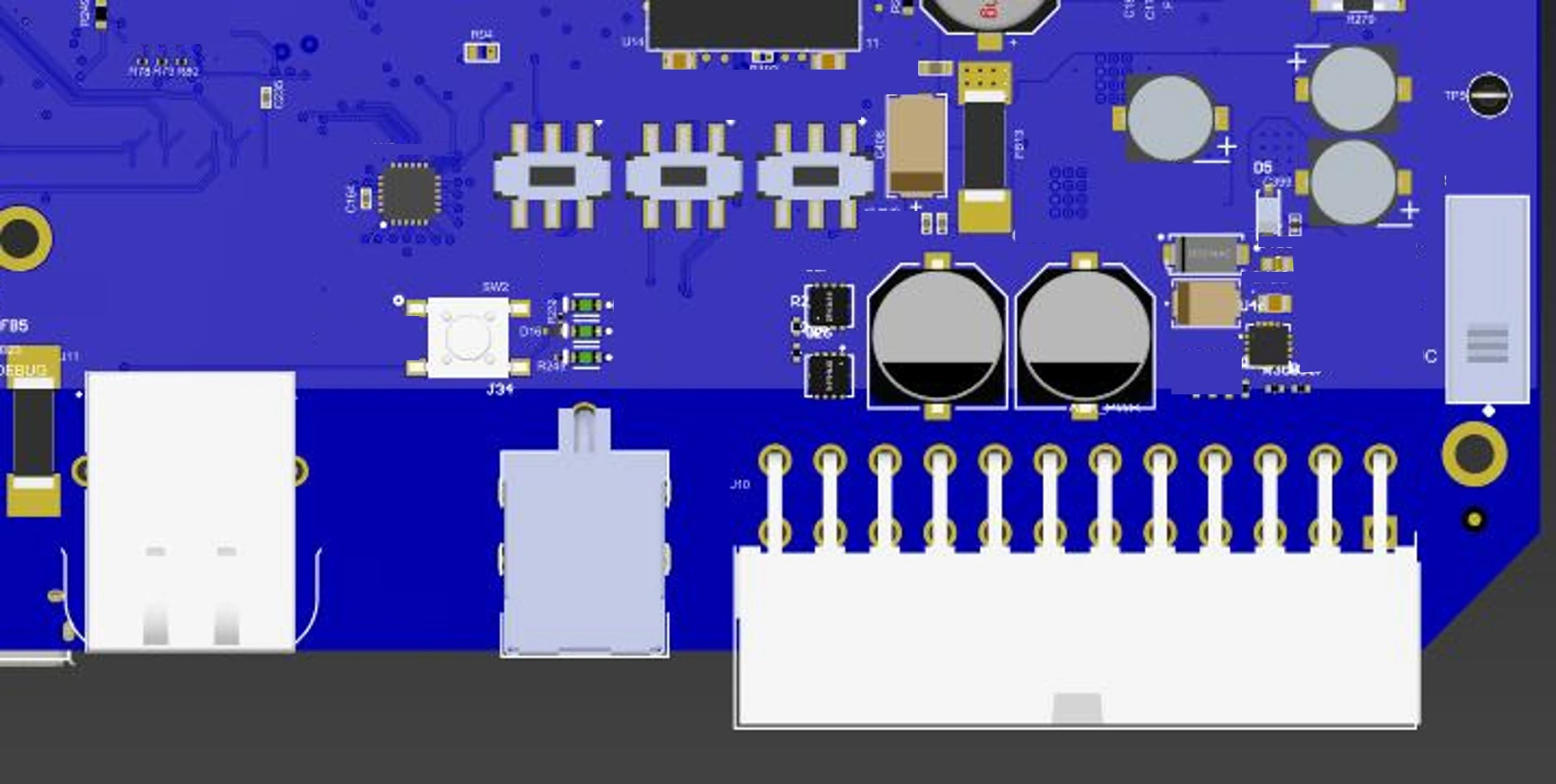
Cable-to-board connectors provide the interface between the PCB and external cables, making them essential for I/O interfaces and high-speed communication ports (e.g., QSFP, SMA, PCIe cables). These connectors must ensure a smooth transition from cable transmission media to PCB traces, which is often a major source of signal degradation.
Key challenges include:
- Impedance mismatch between cable and PCB
- Mode conversion at the transition point
- Launch geometry optimization (especially for coaxial or twinax cables)
- Unlike board-to-board systems, where the environment is controlled, cable interfaces introduce variability due to cable construction, length, and shielding.
At Sierra Circuits, we can build PCBs with ±5% impedance tolerance. We add impedance test coupons to each panel and validate the impedance to ensure it matches your requirements. These test coupons replicate the trace structure and layer stack-up of the actual PCB.

To learn more, see controlled impedance capabilities.
Comparison of high-speed connector types
| Connector type | Typical use case | Data rate capability | Challenge |
|---|---|---|---|
| Board-to-board | Compact modular systems | Up to 112 Gbps | Consumes more space |
| Backplane | Servers, telecom | 56–112 Gbps | High channel loss |
| Wire-to-board | External interfaces | 28–112 Gbps | High transition loss |
The difference between a working design and a failed one often comes down to small details: a stub length, a dielectric mismatch, or a poorly designed launch. By applying the strategies outlined in this article, you can ensure your high-speed designs meet both signal integrity and manufacturability requirements.
High-speed connector design cannot be separated from PCB layout and fabrication. The connector launch, trace geometry, vias, reference planes, return paths, materials, and stack-up all contribute to the electrical behavior of the channel.
A reliable design therefore starts long before the connector is placed on the PCB. Choose the connector based on its electrical characteristics, maintain controlled impedance, provide continuous return paths, minimize via discontinuities, and select low-loss materials. Just as importantly, validate the design against real fabrication capabilities.
About the technical reviewer:
Dilip Kumar is the Senior Design Manager at Sierra Circuits with over a decade of experience in developing high-speed and HDI PCB designs featuring fine-pitch BGAs. He is proficient in Altium Designer, Cadence Allegro, Eagle PCB, KiCAD, and AutoCAD.
Leading a team of skilled PCB designers and layout engineers, he oversees projects from concept to production, ensuring precision and manufacturability at every stage. Dilip consistently delivers innovative, high-quality designs that meet demanding engineering and business objectives.
About Poulomi Ghosh : Poulomi is a microwave engineer specializing in EMI, EMC, RF, and high-speed electronics. As a senior technical writer at Sierra Circuits, she creates advanced engineering articles and webinars for hardware engineers and PCB designers.





Start the discussion at sierraconnect.protoexpress.com