



Contents

On-demand webinar
How Good is My Shield? An Introduction to Transfer Impedance and Shielding Effectiveness
by Karen Burnham
Designing a PCB for electromagnetic compliance starts with identifying and controlling the sources of unwanted EM energy.
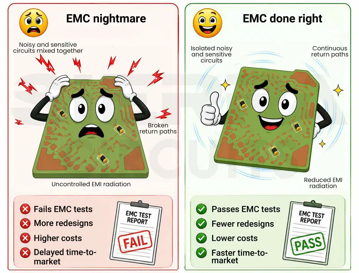
Board designers can achieve electromagnetic compatibility (EMC) by isolating noisy and sensitive circuits, maintaining continuous ground-current paths, and minimizing high-frequency switching-current areas.
Signal integrity engineers should evaluate the circuit board as part of the complete product. They should consider cables, interfaces, power supplies, the enclosure, and other system-level factors that can influence overall performance.
Following these design guidelines can help your product pass essential tests, avoid expensive redesigns, and reach the market faster.
In this article, you will learn how to ensure EMC compliance through stack-up planning, signal and power integrity, and prototype validation.
Highlights:
- Treat EMC as a design objective, not a final testing activity.
- Identify applicable standards early to avoid costly redesigns.
- Define EMC requirements early and incorporate them into architecture, stack-up, component placement, and layout decisions.
- Validate the complete product through EMC-focused design reviews, simulation, prototype measurements, and system-level evaluation.
What is electromagnetic compliance in PCB design?
It is the ability of an electronic product to meet applicable emission and immunity requirements while operating reliably in its intended environment.
Although compliance is verified during product certification, design decisions directly affect the EMC performance of the overall system.
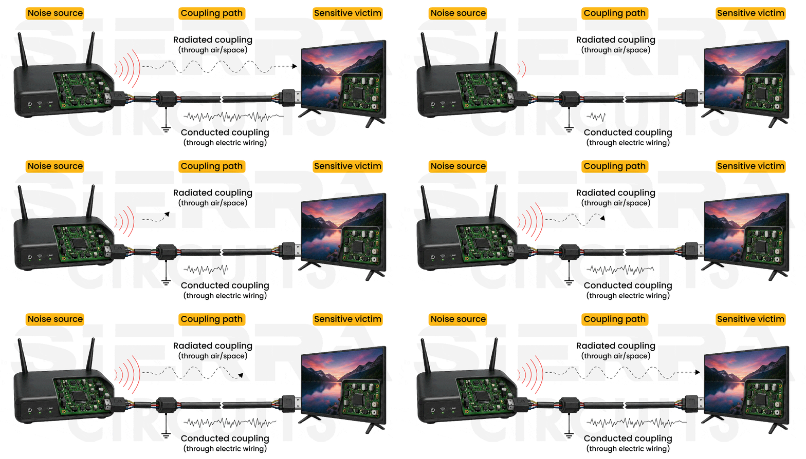
During certification, products are evaluated for radiated and conducted emissions, as well as immunity to disturbances such as electrostatic discharge (ESD), radiated EM fields, and transient events.
For PCB designers, electromagnetic compliance should be considered a design objective rather than a final testing activity.
Decisions related to stack-up, component placement, grounding, reference-current paths, routing, and power distribution play an important role in controlling electromagnetic energy and improving EMC performance before formal compliance testing.
For more, download the EMI and EMC Design Guidelines for PCBs.
EMI and EMC Design Guidelines for PCBs
6 Chapters - 77 Pages - 75 Minute ReadWhat's Inside:
- How electromagnetic interference is generated and spreads
- How to identify EMC requirements and applicable standards
- How to design for electromagnetic resilience
- Common EMI sources: Switching circuits, PWM signals, and motors
- PCB structures that cause radiated emissions
- Practical layout, stack-up, filtering, and shielding guidelines
Download Now
Why should engineers consider EMC early in the design phase?
Designing the system architecture, schematic, and PCB layout with electromagnetic compatibility in mind can significantly improve performance and reduce the need for expensive redesigns if the system fails to meet applicable standards.
Changes introduced during later stages can have a cascading effect across multiple engineering disciplines. For example, relocating a high-speed interface may require updates to the schematic, PCB layout, enclosure, cable assembly, firmware, and manufacturing documentation. Incorporating EMC requirements early helps minimize these redesign cycles and the associated development effort.

What EMC standards apply to your electronic products?
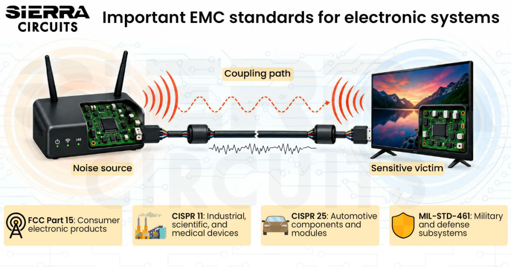
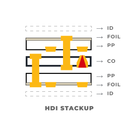
Engineers should identify the applicable EMC benchmarks based on the product’s application, target market, and operating environment. Commonly referenced standards include FCC Part 15, CISPR 11, CISPR 25, CISPR 32, the IEC 61000 series, and MIL-STD-461.
The table below lists some commonly referenced EMC standards for electronic products.
| Standard | Typical application |
|---|---|
| FCC Part 15 | Consumer and commercial electronic products subject to U.S. requirements for intentional, unintentional, and incidental RF emissions |
| CISPR 11 | Industrial, scientific, and medical (ISM) equipment; RF disturbance emission requirements |
| CISPR 25 | Automotive components and modules; specifies limits and measurement methods for radio disturbances that could affect vehicle receivers |
| CISPR 32 | Multimedia equipment (MME), including applicable information and communication technology equipment, for emission requirements |
| IEC 61000 series | Electrical and electronic equipment covering EMC emission, immunity, and testing requirements |
| MIL-STD-461 | Military and defense equipment and subsystems; defines EMC requirements and test methods for conducted and radiated emissions and susceptibility |
Identifying these documents during product planning helps you establish the applicable emission and immunity requirements before schematic design and component selection.
How is electromagnetic compliance evaluated?
EMC is evaluated through standardized tests that assess both emissions from an electronic system and its ability to operate reliably when exposed to disturbances.
Depending on the applicable standards and product category, evaluation may include a combination of emission and immunity tests, as shown below.
| EMC test | What the test evaluates |
|---|---|
| Radiated emissions | Measures electromagnetic energy radiated by the product, typically from 30 MHz to 1 GHz (and higher for some products), to verify emissions remain within regulatory limits. Testing is generally performed in an anechoic or semi-anechoic chamber |
| Conducted emissions | Monitors electromagnetic noise conducted through power or signal cables, typically over the 150 kHz to 30 MHz range, to ensure conducted emissions remain within specified limits |
| Radiated immunity | Evaluates whether the product continues to operate correctly when exposed to controlled RF electromagnetic fields, typically from 80 MHz to 6 GHz, without performance degradation |
| Conducted immunity | Introduces controlled electrical disturbances through power or signal cables to verify the product can continue operating correctly in the presence of conducted interference |
| Electrostatic discharge (ESD) | Simulates electrostatic discharge events (for example, contact and air discharges) to evaluate the product’s ability to withstand static electricity without malfunction or permanent damage |
| Electrical fast transient (EFT) | Reproduces repetitive high-speed switching transients commonly found in industrial power systems to evaluate transient immunity |
| Surge immunity | Applies high-energy surge pulses to power or communication lines to verify the product can withstand lightning-induced or switching-related overvoltage events |
| Voltage dips and interruptions | Assesses whether the product continues to operate correctly during temporary reductions, interruptions, or variations in its supply voltage |
| Power-frequency magnetic-field immunity | Verifies if the product maintains normal operation when exposed to controlled low-frequency magnetic fields |
What design mistakes lead to EMC failures?
Designers should watch out for these common mistakes, as they can increase EMI risks and potentially lead to compliance failures.
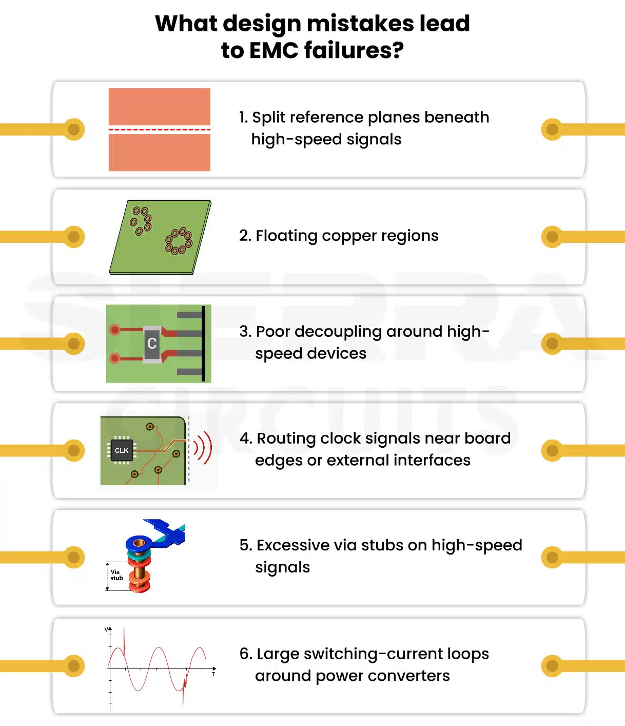
To learn how to reduce electromagnetic interference, see 7 tips and PCB design guidelines for EMI and EMC.
Designer’s checklist for ensuring electromagnetic compliance in PCBs
Use this checklist before releasing the design file for fabrication or formal EMC testing. Resolving EMC risks before prototype fabrication can reduce the likelihood of costly hardware redesigns during later testing.
| No. | Checklist items | ✓ |
|---|---|---|
| PCB architecture and component placement | ||
| 1 | Verify that analog, digital, RF, and power circuits are separated into clearly defined functional zones. | ☐ |
| 2 | Ensure switching regulators, DC-DC converters, and clock circuits are placed away from sensitive analog circuitry. | ☐ |
| 3 | Place crystal oscillators as close as possible to the devices they clock. | ☐ |
| 4 | Position external interfaces close to board-edge connectors to minimize routing length. | ☐ |
| 5 | Place power-management circuits close to their respective loads to reduce switching-current paths. | ☐ |
| 6 | Ensure the selected logic family has no higher switching speed than required. | ☐ |
| 7 | Verify that the IC provides a high noise margin. | ☐ |
| Stack-up and grounding | ||
| 8 | Verify that all high-speed signals have a continuous reference plane, preferably a ground plane. | ☐ |
| 9 | Ensure no critical signals cross split or discontinuous reference planes. | ☐ |
| 10 | Place ground transition vias adjacent to signal vias wherever signals transition between layers. | ☐ |
| 11 | Avoid multiple disconnected ground regions. | ☐ |
| 12 | Verify continuous reference-current paths across the entire PCB. | ☐ |
| Signal routing | ||
| 13 | Maintain controlled impedance for high-speed signals according to interface requirements. | ☐ |
| 14 | Verify differential pairs have matched electrical lengths, consistent spacing, and continuous reference planes. | ☐ |
| 15 | Minimize long parallel routing between high-speed and sensitive signals to reduce crosstalk. | ☐ |
| 16 | Minimize excessive via stubs, unnecessary vias, and unnecessary layer transitions on critical signal paths. | ☐ |
| 17 | Ensure high-speed clocks are routed away from board edges, connectors, and sensitive analog circuitry. | ☐ |
| Power distribution network (PDN) | ||
| 18 | Place high-frequency decoupling capacitors immediately adjacent to IC power pins and provide adequate bulk capacitance where required. | ☐ |
| 19 | Minimize switching-current flow areas around DC-DC converters and power stages. | ☐ |
| 20 | Verify power-entry circuits include appropriate filtering, surge protection, or transient suppression where required. | ☐ |
| 21 | Ensure power and ground planes provide low-impedance current paths. | ☐ |
| 22 | Verify that ferrite beads, capacitors, or other appropriate filters are used to attenuate high-frequency noise on power rails. | ☐ |
| EMI risk assessment | ||
| 23 | Remove floating copper regions and large floating metal structures that may behave as unintended antennas. | ☐ |
| 24 | Evaluate ribbon cables and long external wiring as potential sources of radiated or conducted emissions. | ☐ |
| 25 | Review common-mode current paths, cable grounding, and conducted emission risks. | ☐ |
| 26 | Verify that I/O and mains filters are added. | ☐ |
| 27 | Include feedthroughs and three-terminal capacitors for high-frequency EMI filtering. | ☐ |
| 28 | Ensure that cable shields are properly terminated to minimize EMI coupling. | ☐ |
| 29 | Confirm crosstalk has been minimized through spacing, routing strategy, guard traces, or shielding where appropriate. | ☐ |
Grounding and copper coverage are particularly important when reviewing a circuit board for EMC risks.
During our interview with Daniel Beeker of NXP Semiconductors at PCB West in 2022, he explained:
“Implement a minimum-etch approach to have maximum ground. Connect all the extra copper to the ground using vias. Delete the copper islands if you are unable to connect them to the ground. This will create a pseudo-Faraday cage on your circuit board. The increased copper surface area will help distribute the ESD impulses across the board. This limits EMI as you have reduced the voltage applied to each square centimeter of the board surface.”
Reviewing this checklist before prototype fabrication helps reduce redesign cycles and improves the likelihood of first-pass success during pre-compliance and formal EMC certification testing.
How does prototype validation support EMC?
Prototype testing is the bridge between PCB design and production. It verifies whether the assumptions made during system planning, schematic design, stack-up, component placement, and layout translate into the expected electromagnetic performance.
Design reviews help identify potential EMC risks. Prototype validation confirms whether those risks have been adequately addressed before manufacturing release.
This evaluation should consider the product as a complete system rather than focusing solely on the board. Electromagnetic performance depends not only on the board layout, but also on firmware behavior, enclosure design, cable assemblies, power supplies, connectors, and other system-level interactions.
The table below summarizes the most common activities performed during prototype validation.
| Validation activity | Engineering objective |
|---|---|
| EMC design review and DRC | Verify stack-up, grounding, reference-current paths, routing, filtering, and shielding |
| Signal integrity analysis | Evaluate impedance discontinuities, reflections, crosstalk, and high-speed interfaces |
| Power integrity analysis | Assess PDN stability, transient response, and decoupling effectiveness |
| Electromagnetic simulation | Identify coupling mechanisms and potential radiated emissions |
| EMI source identification | Use near-field probes and spectrum analyzers to locate dominant emission sources before certification |
| System-level validation | Confirm enclosure, firmware, connectors, circuit board cables, power supplies, and external interfaces under representative operating conditions |
Performing these engineering evaluations before regulatory testing improves confidence that the design is ready for production while reducing the likelihood of repeated certification cycles and board redesigns.
Need help resolving potential fabrication issues? Book a meeting with our experts, or call us at +1 (800) 763-7503.
Why should PCB designers evaluate EMC at the system level?
Electromagnetic compatibility is ultimately verified for the complete product, not the circuit board alone. During prototype validation, product designers should confirm that changes outside the printed board have not altered the electromagnetic behavior established during layout.
In addition to the PCB, review:
- Enclosure revisions that affect shielding effectiveness or grounding.
- Connector locations and cable routing, as external cables often behave as unintended antennas.
- Power supply configuration, including converter placement and switching behavior.
- Firmware updates that modify clock frequencies, processor activity, or communication interfaces.
- High-speed interfaces operating under representative system conditions.
- PCB revisions or manufacturing changes that may alter impedance, reference-current paths, or EMC performance.
Evaluating the assembled product helps identify system-level interactions that are difficult to predict from layout alone and reduces the risk of unexpected compliance failures during certification.
Not sure if your stack-up is manufacturable? Schedule a design review with our engineers to validate your design and avoid potential fabrication issues.

How do engineering changes affect electromagnetic compliance?
Engineering changes introduced after validation, including component substitutions, firmware updates, connector relocation, or mechanical revisions, can alter switching behavior, cable interfaces, or shielding effectiveness. These changes should be evaluated to determine whether additional verification is required before manufacturing.
Before releasing manufacturing data, review any changes that may influence electromagnetic performance.
| Engineering change | What should be reviewed? |
|---|---|
| Component substitution | Switching frequency, edge rates, package parasitics, and power consumption |
| Firmware update | Clock configuration, processor activity, interface behavior, and communication patterns. |
| Connector relocation | Cable routing, reference-current paths, filtering, and radiated emissions |
| Mechanical redesign | Enclosure shielding, grounding, ventilation openings, and connector placement. |
| Power supply modification | Switching frequency, transient response, and decoupling strategy. |
| PCB revision or manufacturing change | Stack-up, routing, grounding, impedance, anti-pad dimensions, materials, and fabrication tolerances |
Not every engineering change requires repeating compliance testing. However, any modification that affects high-speed interfaces, grounding, power delivery, external connections, or enclosure characteristics should be reviewed. Determine whether additional simulation, pre-compliance measurements, or engineering validation are required before manufacturing release.
Sierra Circuits fabricates and assembles high-quality circuit boards that follow the requirements of EMC regulatory standards.
To learn more, see our rigid PCB manufacturing capabilities.
Electromagnetic compliance is determined long before a product enters a certification laboratory. Decisions related to system architecture, stack-up planning, grounding, current management, component placement, routing, power distribution, and prototype validation collectively determine whether a printed board is likely to meet regulatory requirements.
By integrating electromagnetic compliance into every stage of PCB development, electronic engineers can reduce redesign cycles, improve first-pass certification success, and build products that are more reliable in real-world operating environments.
About the technical reviewer:
Abhishek Chari is the Team Lead for PCB Design at Sierra Circuits, with 6 years of experience specializing in high-speed PCB layouts and advanced HDI technologies. He possesses deep expertise in leading EDA tools, including Altium Designer, Cadence Allegro, Eagle PCB, and KiCad.
About Pooja Mitra : Pooja Mitra is an electronics and communication engineer. With an experience of over three years in the PCB industry, she creates industry-focused articles that help electrical and PCB layout engineers.






Start the discussion at sierraconnect.protoexpress.com