



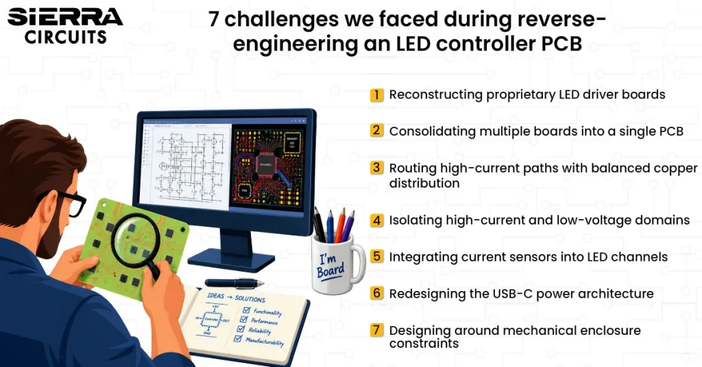
Contents

On-demand webinar
How Good is My Shield? An Introduction to Transfer Impedance and Shielding Effectiveness
by Karen Burnham
Sierra Circuits reverse-engineered an LED controller prototype with multiple off-the-shelf modules and consolidated the design into a single PCB.
The redesigned 4-layer board integrates wireless communication, lighting control, USB-C power delivery, current sensing, and high-current LED switching into a compact form factor.
In this case study, you’ll learn how our designers addressed key engineering challenges, such as power distribution and mixed-signal isolation, to convert a complex prototype into a manufacturable printed board.
Highlights:
To consolidate the prototype into a single printed board, our engineering team:
- Reconstructed proprietary LED driver boards and recreated the schematic.
- Designed a dedicated 24 V power plane for approximately 42 A system current.
- Implemented isolated RS-485 and I²C communication between low-voltage and high-current sections.
- Integrated current sensing devices for 8 LED channels.
- Optimized component placement and copper distribution to fit inside a tapered enclosure.
The LED controller PCB before reverse engineering
The project involved a high-current LED controller developed for wireless lighting applications.
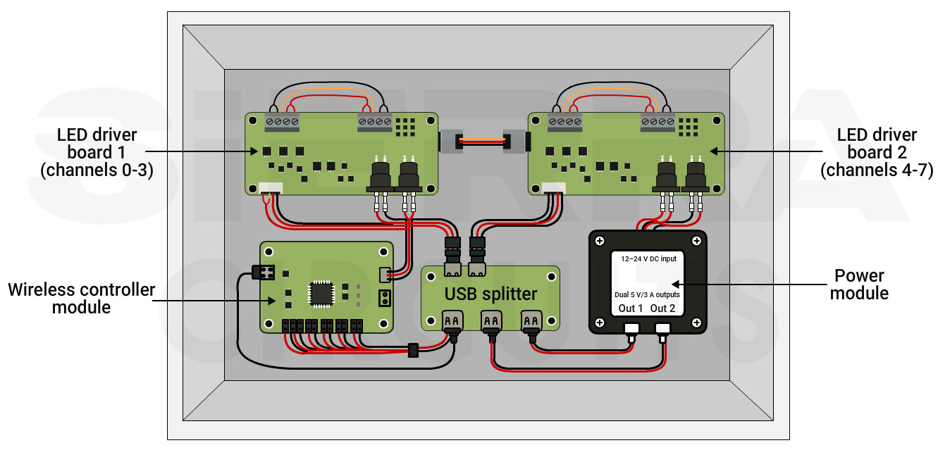
The customer provided a functional prototype assembled using commercially available modules, including:
- Two LED driver boards
- A wireless controller module
- USB-C power boards
- External power module
- Multiple circuit board cable interconnects
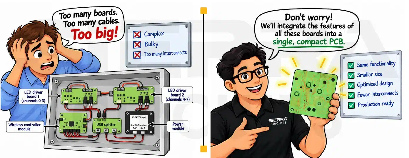
The design team consolidated the multi-board architecture into a single production-ready design, while preserving the validated communication framework and required functionality.
The original prototype used a modular architecture. The wireless controller received commands and transmitted them over RS-485 to 2 LED driver boards. Each driver board controlled 4 LED channels through MOSFET switching stages, providing a total of eight independently controlled channels.
The channels were configured in a daisy-chain architecture:
- Board 1 handled channels 0–3
- Board 2 handled channels 4–7
The RS-485 links were designed with 120 Ω differential impedance to improve noise immunity across inter-board cable connections. Each driver board used onboard address-selection switches for configuring its starting address.
After reverse engineering
The following table summarizes the key specifications of the redesigned LED controller PCB.
| Parameter | Specification |
|---|---|
| Board type | High-current LED controller |
| Layer count | 4 |
| Board dimensions | 3 inches × 10.394 inches |
| Copper thickness | 2 oz on internal layers |
| Input voltage | 24 V |
| Maximum current handling | Approximately 42 A total current |
| Per-channel current capacity | 8A |
| Communication interfaces | RS-485, UART, I²C, USB-C |
| LED outputs | 8 channels |
| Power architecture | Dedicated 24 V power plane |
| Isolation | Isolated RS-485 and I²C communication |
| Mounting | Customer-defined enclosure mounting points |
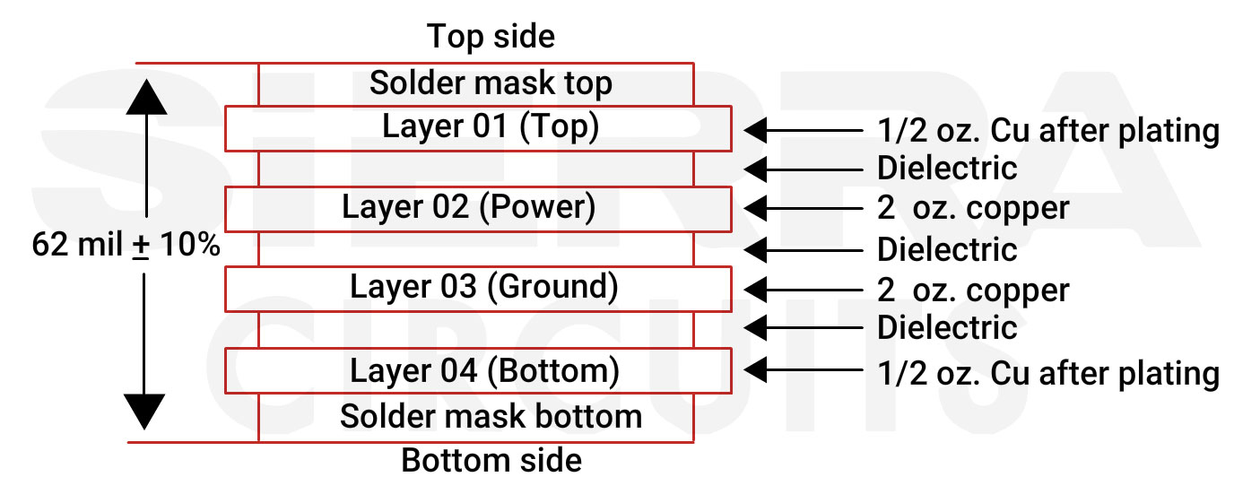
To support the board’s requirements, our designers selected a four-layer PCB stack-up optimized for high-current routing, ground reference continuity for differential pairs, effective heat dissipation, signal integrity, and isolation spacing.
The build-up consisted of:
- Layer 1: Signal routing and MOSFET current paths
- Layer 2: Dedicated 24 V power plane
- Layer 3: Ground reference plane for RS-485 and USB differential pairs
- Layer 4: Differential pair and signal routing
To shorten your product time-to-market, download the Design for Manufacturing Handbook.
Design for Manufacturing Handbook
11 Chapters - 96 Pages - 90 Minute ReadWhat's Inside:
- Annular ring sizes to avoid drill breakouts
- DFM strategies for designing reliable vias
- Trace width and spacing best practices
- Solder mask and silkscreen must-knows
Download Now
How we reverse-engineered the LED controller prototype
The objective of this project was to reverse-engineer the prototype architecture and consolidate the complete system into a single manufacturable PCB.
Here are the hurdles we encountered and the solutions to fix them.
Challenge #1: Reconstructing proprietary driver boards
The customer’s prototype used third-party LED driver boards with unidentified microcontrollers. The controller markings had been removed, and the embedded firmware could not be extracted.
Without access to the original firmware, replacing the controllers with a new MCU would require redevelopment of the complete communication architecture.
This introduced risks related to functional compatibility, communication timing, and system reliability.
Solutions:
Sierra’s PCB designers reverse-engineered the complete architecture of proprietary third-party LED driver hardware by:
- Performing X-ray analysis and physical inspection
- Tracing the schematic
- Identifying component values
- Reconstructing MOSFET driver sections
- Recreating package footprints
- Rebuilding the circuitry in schematic form
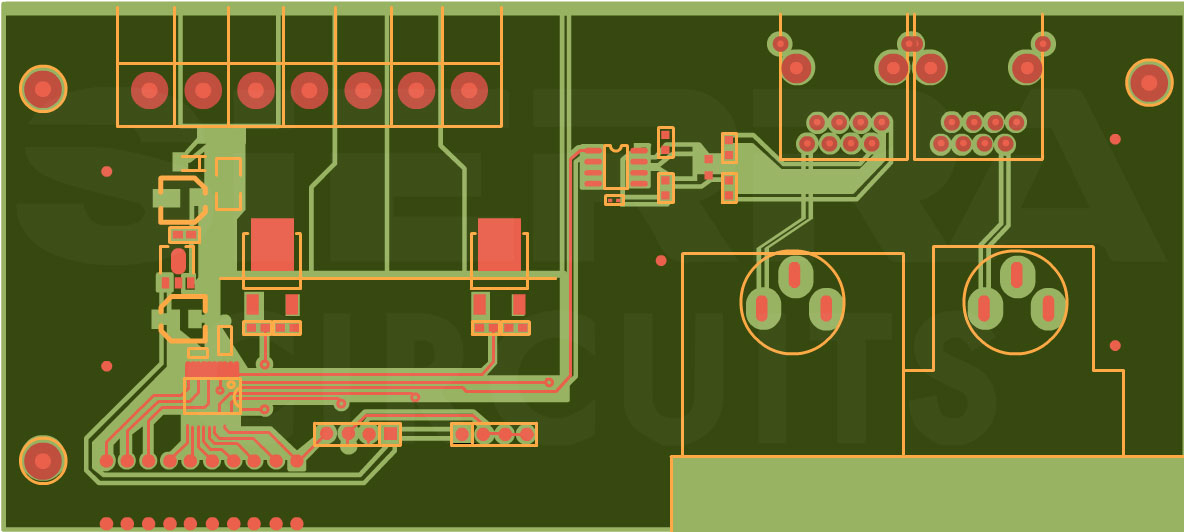
The reconstructed circuitry preserved the validated controller architecture, RS-485-to-UART communication, and channel-addressing scheme. Custom footprints were also created for the unidentified controller packages using physical measurements.
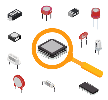
The team identified alternate components for obsolete and unavailable devices while maintaining compatibility with the validated prototype design.
Are you worried about getting low-quality/counterfeit components, price inflation, and inefficient inventory management? We’ve got you covered. Sierra Circuits’ customer-owned inventory services (COIN) is a personalized component sourcing and stocking program designed to meet your specific needs.
With COIN, we procure and store the required parts for your PCBAs, eliminating the risk of counterfeit or low-quality components while ensuring you have access to the necessary parts when you need them.
See our FAQs on COIN services.

Challenge #2: Consolidating multiple boards into a single PCB
The original prototype relied on multiple interconnected boards, external cable assemblies, daughter boards, and power modules to implement the complete LED controller.
This increased assembly complexity, the potential for wiring errors, mechanical instability, and long-term reliability risks. The multi-board architecture also occupied significant enclosure space.
Solutions:
The modular prototype was consolidated into a single PCB while preserving the validated communication architecture and original functionality. This approach also minimized redevelopment risks associated with the proprietary controller firmware.
The redesigned board integrated the following functions:
- Wireless MCU connectivity
- RS-485 communication
- USB-C charging
- Current sensing
- LED driver circuitry
- Power regulation
- Isolation circuitry
The wireless communication module, based on an off-the-shelf controller board, was mounted directly onto the board using dedicated headers. The redesign reduced the number of inter-board connectors from 6 to 2 by replacing cable interconnects with direct PCB routing.
Unused prototype features, including Ethernet connectivity and redundant RGB connector interfaces, were removed from the final architecture to simplify routing and reduce circuit board area. This eliminated unnecessary wiring and improved manufacturability.
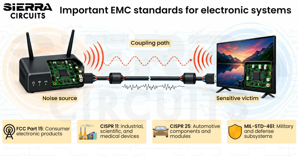
Sierra Circuits fabricates and assembles high-quality circuit boards that follow the requirements of EMC regulatory standards.
To learn more, see our rigid PCB manufacturing capabilities.
Challenge #3: Routing high-current path with balanced copper distribution
The circuit board was designed to support:
- Up to 8 A per output channel
- Approximately 42 A total system current
- High-current MOSFET switching
Distributing this level of current inside a compact board created significant thermal management and copper distribution challenges.
Solutions:
Our layout engineers implemented the following routing strategy:
- A dedicated layer 2 polygon plane for 24 V power distribution
- Wide copper pours for current distribution
- Single-plane 24 V current distribution to avoid excessive current splitting across multiple layers
- 2 oz copper on internal layers
- Distributed current paths on top and bottom layers
- Thermally optimized component placement
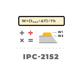
The team analyzed current flow paths, copper distribution, and trace-width requirements throughout the PCB. The dedicated 24 V plane provided a continuous high-current distribution path and helped accommodate the approximately 42 A total system current within the available board area.
Initial current calculations showed that the original board width of approximately 2.5 inches was insufficient to maintain the required trace widths for carrying approximately 21 A through this section. After discussing the constraint with the customer, the board width was increased to 3 inches, providing additional routing space while maintaining the required current-carrying capacity.
Component placement and copper distribution were optimized based on current flow profiles and thermal load across the board.
Dilip Kumar, Senior Design Manager at Sierra Circuits, explained, “Copper imbalance often starts with poor stack-up and layer planning. Random allocation of power and ground layers, placing ground planes too far from signal layers, failing to provide proper reference planes, and routing high-speed signals without considering their specific layout requirements can all lead to uneven copper distribution. These practices can create significant differences in copper density across the board, increasing the risk of manufacturing and signal integrity issues.”
Challenge #4: Isolating high-current and low-voltage domains
The design included:
- High-current LED switching circuitry
- Sensitive wireless MCU circuitry
- Differential communication interfaces
Without proper isolation, electrical faults and switching noise from the high-current LED driver section could propagate into the low-voltage control circuitry.
Solutions:
Our designers developed a partitioned mixed-signal architecture that electrically and physically separated the high-current power stage from the low-voltage control and communication circuitry.
The design implemented galvanic isolation for:
- RS-485 communication paths
- I2C communication lines
- Power supply circuitry
The PCB layout established dedicated isolation boundaries between the high-current MOSFET switching section and the low-voltage communication circuitry.
Power circuitry was positioned on the opposite side of the low-voltage communication section to minimize noise coupling. The low-voltage section incorporated separate analog and digital ground regions to improve noise isolation and signal integrity.
This architecture protects the wireless controller circuitry from faults originating in the high-current LED driver section.
Need assistance in getting your board fabricated? Book a meeting with our experts, or call us at +1 (800) 763-7503.
Challenge #5: Integrating current sensing into each LED channel
The original customer’s prototype did not support current monitoring.
The customer requested independent current sensing for all eight LED channels. However, routing multiple sensing connections into a centralized monitoring circuit would increase routing congestion and placement complexity.
Solutions:
Our engineers selected distributed current sensing ICs and placed them close to each MOSFET channel.
Abhishek Chari, PCB Design Team Lead at Sierra Circuits, explained, “If you have multiple high-current channels, placing a separate current-sensing IC close to each channel can help avoid a centralized star connection and save board space”.
This approach helped in:
- Reducing sense-trace length
- Simplifying component placement
- Improving measurement accuracy
- Minimizing routing congestion
The sensing ICs communicated with the MCU through isolated I2C communication.
The selected current sensing integrated circuits supported a 500 kHz sampling frequency, making them suitable for monitoring PWM-controlled LED channels.
Challenge #6: Redesigning the USB-C power architecture
The old prototype used separate USB-C daughter boards for MCU power delivery, external charging, and USB programming.
The redesign required all these functions to be integrated into the printed board.
Solutions:
Our designers recreated the functionality of the original USB-C modules directly on the PCB, eliminating unnecessary connector interfaces.
The circuitry was redesigned to convert 24 V input to dual 5 V outputs, supply power to the wireless MCU, support USB-C charging, and enable USB programming connectivity
The power section incorporated:
- Dual 5 V/3 A outputs derived from the 24 V input
- Separate power paths for MCU operation and external-device charging
- USB differential pair routing with proper ground reference
- A USB Type-C PMIC configured to advertise 3 A charging capability through the CC pins
The USB regulator section was positioned near the lower region of the PCB to optimize current distribution and reduce routing congestion.
To learn how to develop a circuit board prototype, see building a PCB prototype from scratch: a designer’s guide.
Challenge #7: Designing around mechanical enclosure constraints
The original design had an enclosure with fixed mounting locations, tapered geometry, and non-uniform height restrictions. The enclosure geometry created a narrow routing region that limited the available copper area for the high-current power paths.
These constraints limited placement flexibility and routing space.
Solutions:
We imported the customer-provided enclosure model and used its mechanical geometry to optimize board dimensions, mounting-hole locations, connector placement, and component height distribution.
The final placement ensured sufficient routing clearance while accommodating the enclosure’s height restrictions.
Our engineers balanced electrical, thermal, and mechanical constraints simultaneously, optimizing current paths, component heights, board-to-connector interfaces, and isolation boundaries within the available enclosure space.
Not sure if your stack-up is manufacturable? Schedule a design review with our engineers to validate your design and avoid potential fabrication issues.

Through the collaborative efforts of our schematic, hardware, and PCB layout designers, we reverse-engineered a multi-board LED prototype into a compact, production-oriented embedded system.
About the technical reviewer:
Abhishek Chari is the Team Lead for PCB Design at Sierra Circuits, with 6 years of experience specializing in high-speed PCB layouts and advanced HDI technologies. He possesses deep expertise in leading EDA tools, including Altium Designer, Cadence Allegro, Eagle PCB, and KiCad.
About Pooja Mitra : Pooja Mitra is an electronics and communication engineer. With an experience of over three years in the PCB industry, she creates industry-focused articles that help electrical and PCB layout engineers.





Start the discussion at sierraconnect.protoexpress.com