


Contents

On-demand webinar
How Good is My Shield? An Introduction to Transfer Impedance and Shielding Effectiveness
by Karen Burnham
Designing high-power PCBs with fabrication and assembly in mind will make your manufacturer glad to work with you. Clearly communicating your requirements in the fab and assembly notes might even make you their favorite customer.
PCB designers can make this process easier by designing within the CM’s capabilities and accounting for process limitations from the start.
Highlights:
- Include copper weights, stack-up details, plating requirements, and via filling specifications in fab notes.
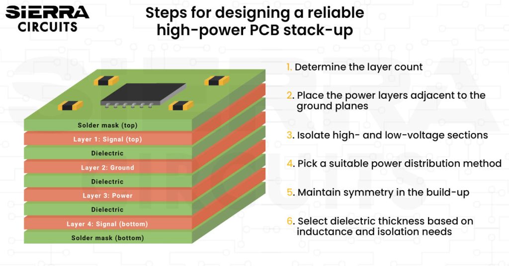
- Use a symmetric, copper-balanced build-up and confirm sequential lamination parameters during the DFM review.
- Incorporate thermal relief pads for component leads connected to large copper planes.
- Optimize pad design, stencil apertures, and via structures for heavy-copper assemblies to minimize solder wicking, voiding, and cold joints.
In this article, you’ll learn how to identify the design mistakes that lead to defective boards and apply best practices to reduce fabrication and assembly flaws.
Addressing fabrication challenges in your high-power PCB designs
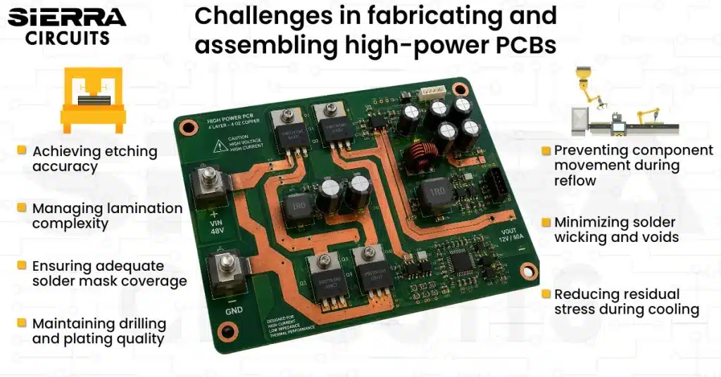
The main hurdles include achieving etching accuracy, managing complex lamination, ensuring sufficient solder mask coverage, and maintaining drilling and via plating quality.
Let’s look at each of these in detail and the design practices to overcome them.
Achieving etching accuracy
As copper thickness increases, it gets harder to etch due to the sidewall undercut. The etchant removes copper laterally beneath the resist, resulting in narrower traces than intended.
To compensate for this effect, fab houses apply etch compensation (positive artwork bias) by increasing the trace width in the design data.

Design recommendations to avoid etching flaws:
- Verify the minimum trace width and spacing supported for heavy copper with your fabricator.
- Avoid very fine features when using copper weights above 3 oz.
- Increase trace clearance to accommodate etching tolerances.
- Discuss etch compensation requirements before finalizing the design.
Managing lamination complexity
Thick copper and high-Tg materials require longer lamination cycles than standard PCB constructions. If the high-load stack-up is not designed correctly, these conditions can lead to resin starvation, void formation, and excessive Z-axis expansion.
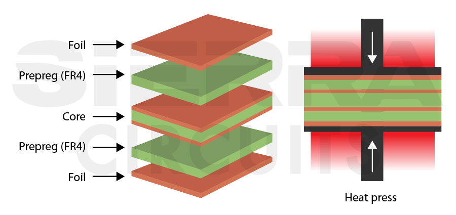
Copper imbalance across the stack-up further increases mechanical stress during lamination and can cause board warpage.
Here’s how you can ensure reliable lamination:
- Use a symmetric, copper-balanced build-up and confirm sequential lamination parameters during the DFM review.
- Avoid concentrating heavy copper on one side of the PCB.
- Utilize high-resin content prepregs (like 1080 or 2116) or resin-coated copper (RCC) to completely fill the voids between thick traces.
To learn how to build a high-load board, download the High-Power PCB Design Guide.

High-Power PCB Design Guide
12 Chapters - 96 Pages - 75 Minute ReadWhat's Inside:
- Guidelines for designing traces, planes, and vias for high current
- Material selection, stack-up, and power distribution strategies
- Thermal management techniques for power electronics
- Creepage and clearance rules based on the industry standards
- Common design mistakes and how to avoid them
Download Now
Ensuring adequate solder mask coverage
Applying solder mask over heavy copper is more difficult due to steep copper sidewalls. Poor coverage can expose copper, reduce insulation, and increase the risk of contamination and corrosion.
Some high-current designs intentionally expose copper to improve thermal performance. These openings should be defined deliberately rather than occurring as a manufacturing issue.
To improve solder mask reliability:
- Avoid narrow solder mask dams between thick copper features.
- Maintain sufficient spacing between high-current conductors.
- Use solder mask-defined (SMD) pads where appropriate for large copper areas.
- Review solder mask requirements with the fabricator during the DFM review.
To learn the typical causes of high-load board fabrication failure, see why your high-power PCBs fail: 3 main reasons.
Maintaining drilling and plating quality
High-power PCB fabrication often combines thick laminates with relatively small vias, creating high aspect-ratio holes that are more difficult to drill and plate.
Drilling circuit boards with multiple heavy copper layers increases drill wear and the likelihood of hole deflection and resin smear. These factors make it harder to achieve uniform plating inside the via barrel, increasing the risk of thin plating, voids, higher electrical resistance, and premature via failure during thermal cycling.
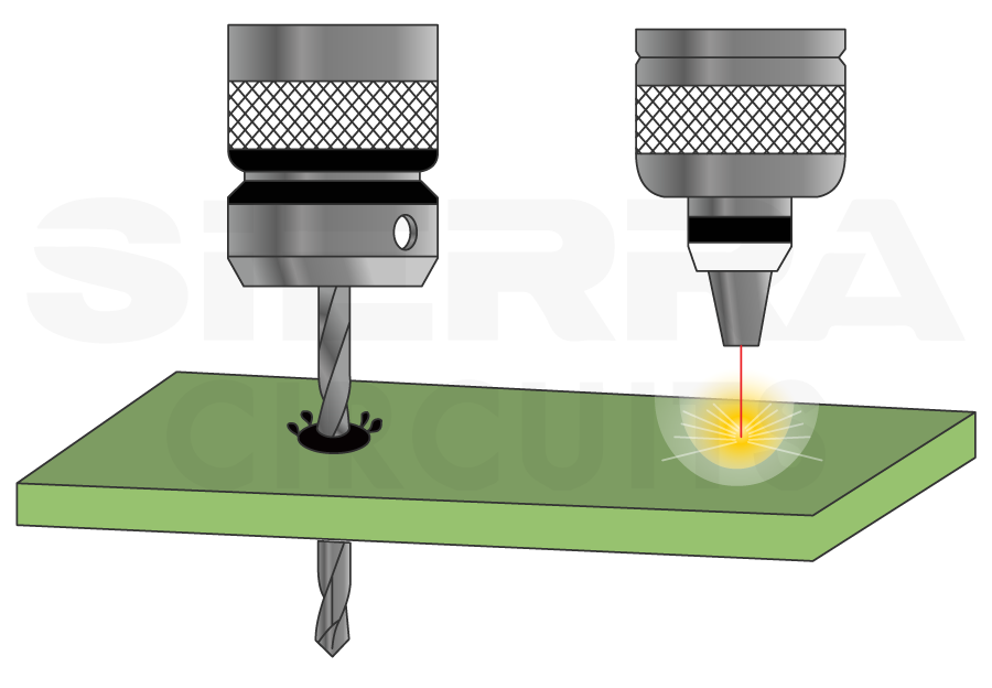
Follow these design practices to improve via reliability:
- Keep the aspect ratios between 6:1 and 8:1.
- Increase via diameter as the board thickness increases.
- Use multiple vias in parallel instead of relying on a single via for high-current transitions.
- Specify 1.5–2 mil barrel plating or filled vias for high-current paths.
- Confirm drilling capabilities and plating requirements with the fabricator during the DFM review.
Successful high-power PCB fabrication depends on understanding these constraints early in the design process.


What design mistakes lead to fabrication issues in high-load printed boards?
Most fabrication issues arise from design decisions that exceed the fabricator’s capabilities or from incomplete manufacturing documentation. These mistakes can delay production and reduce yield.
| Mistake | Consequence | How to prevent it |
|---|---|---|
| Specifying copper weight without considering etch compensation | Narrower traces after etching, reducing current-carrying capacity | Discuss etch compensation with the fabricator. Include compensation in the design or allow the CM to adjust it during fabrication. |
| Designing traces with incompatible width and spacing for heavy copper | Etch bridging, short circuits, and scrapped panels | Verify the fabricator’s minimum trace width and spacing for the selected copper weight, and increase them if necessary. |
| Using high-aspect-ratio vias without consulting the fabricator | Plating voids and unreliable vias | Keep the aspect ratio between 6:1 and 8:1. For higher ratios, use blind/buried vias or larger drill diameters. |
| Missing or incomplete fabrication notes | Misinterpretation, production delays, and incorrectly built boards | Provide detailed fabrication notes covering stack-up, materials, copper weights, via filling, solder mask, and testing requirements. |
| Not specifying via filling for vias under pads | Solder wicking, voided joints, and open circuits | Specify IPC-4761 Type VII (filled and capped) for all vias located under component pads. |
| Using a standard solder mask over heavy copper without verification | Thin mask coverage and peeling during soldering | Ask your fabricator to use an LPI solder mask designed for heavy-copper boards. Consider thicker mask coverage or mask relief for tall copper features. |
| Insufficient stack-up and copper balance documentation | Warpage and layer-to-layer registration issues | Provide a detailed stack-up diagram showing material types, dielectric thicknesses, and copper weights. Specify symmetry requirements where applicable. |
At Sierra Circuits, we perform thorough DFM checks on spacing, build-up, and via structures before fabrication begins. This helps us identify potential manufacturing risks and deliver high-quality circuit boards.
For more, see our rigid PCB manufacturing capabilities.
Addressing assembly challenges in your high-power PCBs
High-load assemblies require modified soldering processes because heavy copper, large thermal masses, and high-load components heat and cool differently than those on standard boards. As a result, convention assembly methods may not produce reliable solder joints.
If these factors aren’t considered, they can lead to solder defects, component movement, residual mechanical stress, and long-term reliability issues.
Here are the challenges in assembling high-power printed boards:
Preventing component movement during reflow
Large inductors, transformers, TO-247 packages, and high-current connectors can shift during reflow because molten solder may not adequately support their weight.
Heavy copper planes also create uneven heating across the circuit board, which can lead to uneven solder wetting, increasing the risk of tombstoning in small devices and component movement in larger parts.
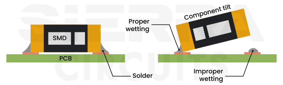
To avoid such issues:
- Follow the component manufacturer’s recommended land pattern.
- Provide sufficient mechanical support for large or vibration-sensitive parts.
- Discuss the use of temporary adhesive dots or mechanical fixtures with your assembly house.
- Ask your CM to optimize the reflow profile for assemblies with large thermal masses.

Minimizing solder wicking and voids
Large thermal pads containing unfilled via arrays can draw solder away from the component pins through capillary action (wicking), creating starved joints. Additionally, large surface-area power pads easily trap outgassing flux volatiles, resulting in high percentages of solder voiding that diminish both electrical and thermal conductivity.
Heavy copper planes also act as heat sinks during reflow, absorbing thermal energy from nearby solder joints. Without adequate thermal balancing, this can lead to incomplete solder wetting, cold joints, or inconsistent solder fillets.
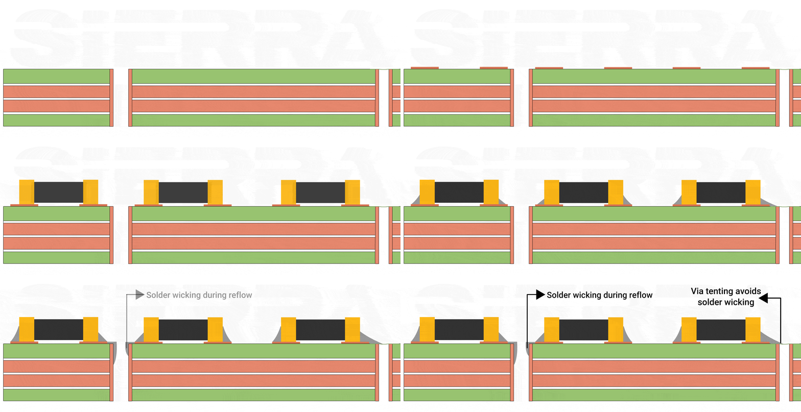
To ensure solder joint quality:
- Use SMD pads to better control solder spread on large thermal pads.
- Specify filled and capped vias beneath large thermal pads to reduce solder wicking.
- Incorporate thermal relief pads for component leads connected to large copper planes, unless they carry high current.
- Design stencil apertures to deliver the appropriate solder volume for large thermal pads.
- Discuss solder paste selection and reflow profile requirements with your assembly house.
Need help resolving potential assembly issues? Book a meeting with our experts, or call us at +1 (800) 763-7503.
Reducing residual stress during cooling
Heavy-copper boards cool more slowly than standard ones because thick copper retains heat for longer periods. This creates residual mechanical stress that can contribute to solder-joint fatigue, via cracking, and reduced reliability during thermal cycling.
Design recommendations to minimize residual stress:
- Maintain balanced copper distribution across the PCB to minimize thermal gradients.
- Ask your assembly house to implement controlled ramp-down cooling after reflow.
- Request cross-section analysis during first-article builds to verify solder joint and via quality.
- Discuss solder alloy selection with your CM for applications exposed to frequent thermal cycling or elevated operating temperatures.
For more, download our PCB Design for Assembly Handbook.
PCB Design for Assembly Handbook
6 Chapters - 50 Pages - 70 Minute ReadWhat's Inside:
- Recommended layout for components
- Common PCB assembly defects
- Factors that impact the cost of the PCB assembly, including:
- Component packages
- Board assembly volumes
Download Now
What design mistakes lead to assembly defects in high-load boards?
Assembly errors often occur when the design doesn’t account for the thermal mass of heavy copper boards or when manufacturing requirements aren’t clearly specified.
These oversights can affect soldering, component placement, cleaning, and protective coating, reducing assembly quality and long-term reliability.
| Mistake | Consequence | Prevention |
|---|---|---|
| Omitting thermal relief for non-power pads connected to large copper planes | Tombstoning and poor solder joints | Use thermal relief for pads that are not part of the primary current path. For power pads, optimize the stencil design and reflow profile instead. |
| Not providing mechanical support for heavy components | Solder joint fatigue and component detachment under vibration | Use adhesives, clips, or brackets to secure large inductors, transformers, and other heavy components. |
| Not specifying conformal coating | Creepage failures and corrosion | Specify conformal coating type (acrylic, silicone, parylene) and cleaning process in assembly notes. |
| Placing vias beneath large SMD components without proper treatment | Via damage during reflow and solder wicking | Use filled and capped vias (IPC-4761 Type VII) under components, and ensure the surface is planar for reliable mounting. |
| Designing pads and stencil openings without considering the thermal mass of heavy copper | Incomplete solder joints, cold joints, and inconsistent solder wetting | Optimize the stencil aperture design and ask your CM to develop an appropriate reflow profile for heavy-copper assemblies. Verify solder joint quality during prototype builds. |
Need help in designing reliable high-power PCBs? Our engineering team can help you with thermal management, stack-up design, and DFM analysis.

What should you include in your high-power PCB fabrication and assembly notes?
It should specify all fabrication and assembly requirements that cannot be inferred from the design files, such as the stack-up, copper weights, via specifications, surface finish, assembly processes, and inspection requirements.
Clearly documenting these details helps prevent quotation delays, engineering queries, fabrication, and assembly errors.
| Fab notes | Assembly notes |
|---|---|
| Copper weight for every layer | PCB bill of materials with valid manufacturer part numbers (MPNs) and clearly identified DNI components |
| Approved board thickness and stack-up | Pick-and-place (centroid) files and assembly drawings |
| Minimum via plating thickness and any via filling or capping requirements | Mechanical support requirements for heavy or vibration-sensitive components |
| Heavy-copper regions, bus bars, edge plating, or other special fabrication features | Conformal coating, selective soldering, underfill, or other special assembly processes |
| Surface finish, solder mask type and color, and required IPC class | X-ray inspection requirements for solder voiding on large thermal pads |
| Electrical test requirements and controlled impedance specifications (if applicable) | Cross-section analysis requirements for first-article builds |
High-power PCB fabrication and assembly require more than selecting heavy copper or increasing board thickness. Every design decision influences manufacturing yield and long-term reliability.
Addressing manufacturing and assembly constraints during the design stage helps you prevent production delays, reduce defects, and improve product reliability. An early DFM review can identify design issues that could affect fabrication yield and assembly reliability.
About the technical reviewer:
Dilip Kumar is the Senior Design Manager at Sierra Circuits with over a decade of experience in developing high-speed and HDI PCB designs featuring fine-pitch BGAs. He is proficient in Altium Designer, Cadence Allegro, Eagle PCB, KiCAD, and AutoCAD.
Leading a team of skilled designers and layout engineers, he oversees projects from concept to production, ensuring precision and manufacturability at every stage. Dilip consistently delivers innovative, high-quality designs that meet demanding engineering and business objectives.
About Mohamed Faheemuddin : Mohamed Faheemuddin is a mechanical engineer. His passion for electronics drew him to the PCB industry. With an experience of over 3 years in the PCB industry, he specializes in developing articles for engineers and hardware designers.






Start the discussion at sierraconnect.protoexpress.com