


Contents
High-power PCBs fail when current-induced heating, voltage stress, and mechanical strain exceed the design limits. These problems are often caused by poor design decisions, including layout planning, stack-up, and thermal management. This can lead to overheating and long-term structural damage.
Board designers and power electronics engineers should optimize thermal paths, maintain adequate creepage and clearance, balance copper distribution, and validate designs under real operating conditions to avoid board failures.
In this article, you will learn the 3 common causes of high-power PCB failure and the design techniques to prevent thermal, electrical, and mechanical issues.
Highlights:
- Design high-current traces using IPC-2152 guidelines, apply current derating, and use copper pours or busbars to reduce excessive heating.
- Select high-CTI laminates to prevent arcing and insulation breakdown.
- Implement balanced stack-ups to reduce the risk of board warpage.
- Incorporate thermal vias, heat-spreading copper planes, and low-resistance thermal interface materials to improve heat dissipation in power components.
At high current levels, even small resistances generate significant heat (P = I²R). As temperature increases, copper resistance rises (~0.39%/°C), further accelerating heat generation and pushing the system toward thermal breakdown. At the same time, high voltage introduces electric fields that can cause insulation breakdown, arcing, and long-term material degradation.
Here are 3 main reasons and preventive techniques.
1. Poor thermal management leads to solder fatigue and overheating
Heat accumulation increases conductor resistance, accelerates dielectric material aging, and weakens electrical interconnects.
Thermal issues are one of the most common reasons for high-power PCB failure since every high-current path generates heat through resistive losses.
PCB temperature increases due to:
- Joule heating in conductors
- Switching and conduction losses in semiconductors
- Dielectric and parasitic losses at high frequency
If this heat is not efficiently dissipated, it accumulates, raising the overall board temperature and degrading materials. Components operating above their rated junction temperature experience shorter lifetimes and reduced efficiency. Localized hotspots can also damage copper traces and weaken laminate adhesion.
Design techniques to prevent solder fatigue in high-power PCBs
Repeated temperature cycling causes solder joints to expand and contract. Large thermal pads and heavy components experience higher mechanical stress. Over time, cracks form inside the solder structure. This issue becomes more severe in automotive, aerospace, and industrial equipment with continuous temperature cycling.

Stick to the following guidelines to reduce the risk of solder fatigue:
- Match the component package CTE with the laminate properties, and select packages with low thermal resistance.
- Follow IPC class 3 assembly requirements for mission-critical products.
- Avoid uneven copper distribution around large thermal pads.
- Perform accelerated thermal cycling tests during validation.
How to reduce PCB trace heating
Undersized copper traces generate excessive losses under high current. Rising temperature further increases resistance, accelerating heating and potentially leading to failure in high-power PCBs.
To reduce excessive heating in traces:
- Use IPC-2152 standard charts to model your trace widths.
- Add a 20 – 30% current derating margin.
- Verify trace width at worst-case ambient temperature.
- Avoid narrow sections (current bottlenecks).
- Split the current across parallel traces where needed.
- Remove solder mask over high-current copper where additional cooling is required, ensuring insulation and oxidation risks are addressed.
- Route high-current paths on outer layers where possible, as external layers dissipate heat more effectively because convection improves cooling.
- Use copper pours and planes for very high-current rails. Transition to busbars when the required trace width becomes impractical (often in very high current designs, e.g., ~100 A and above).

To learn how to design efficient traces, download the PCB Trace and Space Handbook.
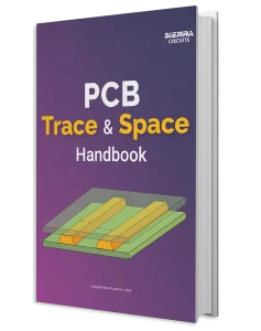
PCB Trace and Space Handbook
8 Chapters - 34 Pages - 40 Minute ReadWhat's Inside:
- Key factors influencing line width and spacing
- Clearance guidelines for high-voltage and high-speed traces
- DFM rules for heavy copper PCBs
- Via considerations
- Industry standards for trace and space design
Download Now
How to improve heat dissipation in power components
Insufficient thermal paths hinder heat dissipation and prevent the cooling of power devices. MOSFETs, regulators, IGBTs, and power modules can exceed their junction temperature limits if heat sinks and thermal interfaces are poorly designed.
Follow the tips below for better heat dissipation:
- Place thermal via arrays under exposed pads to improve heat transfer into inner layers.

A thermal via array is added under the component’s pad to increase the heat dissipation. - Select heat sinks based on worst-case power dissipation, not nominal conditions.
- Leverage large copper planes to spread heat and reduce hotspots.

Heat dissipation through copper planes in a PCB. - Connect high-power component thermal pads directly to copper pours; avoid thermal relief spokes for power pads.
- Use via stitching to connect copper layers.
- Choose low-resistance thermal interface materials (TIM).
- Verify airflow and cooling under actual enclosure conditions.

Strategies to avoid delamination in high-power PCBs
Excessive thermal stress can separate laminate layers and create internal voids. Heavy copper designs and high operating temperatures increase the risk of delamination. Repeated thermal cycling also weakens resin bonding.

Modern laminates resist delamination better than older materials. However, continuous operation near glass transition temperature (Tg) still reduces reliability.
- Select laminates with a Tg at least 20 – 25 °C above the operating temperature.
- Upgrade to high-Tg FR4 for temperatures above 100-110 °C.
- Use polyimide materials in extreme thermal environments.
- Avoid prolonged operation near Tg limits. Consider ceramic or metal-core printed boards when thermal limits are exceeded.
- Balance copper distribution across layers.
For more tips on heat dissipation, see 12 PCB thermal management techniques to reduce heating.
2. Insulation breakdown causes arcing and voltage instability
Voltage stress causes insulation failure when conductor spacing is inadequate and material properties are incompatible. High-voltage designs require sufficient creepage, clearance, and dielectric coordination. Moisture, contamination, and sharp conductor geometries further increase the breakdown risk.
Spacing guidelines to prevent arcing in high-power PCBs
Excessive electric fields can ionize air between conductors. This creates arcing through the air gap or carbonized tracking paths across the board surface.
Follow the tips below to reduce arcing risks:
- Maintain sufficient creepage and clearance.

- Follow IEC 60664-1 or IPC-2221 to calculate conductor spacing requirements for electrical insulation.
- Add a slot between traces or place vertical insulation barriers. Incorporating a V-groove, parallel-sided notch, or placing a slot in your design can solve creepage issues.

Slots, grooves, and notches increase creepage in the PCB layout. - Increase spacing near high-voltage connectors.
- Avoid routing high-voltage nets near board edges.
- Use materials with CTI ≥ 400 V above 300 V DC. Higher CTI improves resistance to moisture-induced tracking.
- Apply coating in polluted or high-humidity environments. This minimizes leakage current caused by contamination.
Need help in designing reliable high-power PCBs? Our engineering team can help you with thermal management, stack-up design, and DFM analysis.
You can book a meeting with our experts or call us at +1 (800) 763-7503.

Routing strategies to minimize voltage drops
Even small resistances can cause a significant voltage drop in high-current paths. Long conductors and narrow traces further increase resistive losses. This reduces system efficiency and can degrade power regulation and voltage stability. It also increases power dissipation, leading to additional heating. In severe cases, it can contribute to high-power PCB failure by increasing thermal stress and overstressing components and power delivery networks.
To prevent voltage drops:
- Keep current paths short and wide.
- Increase trace width beyond thermal minimums.
- Use dedicated power planes for high-current rails.
- Reduce unnecessary connector transitions.
- Verify voltage drop during power integrity analysis.
If the voltage drop exceeds 1 – 2% of the rail voltage, increase the conductor cross-sectional area.
Design practices to reduce partial discharge
Partial discharge occurs when localized electric fields ionize small air gaps or voids inside insulating materials, gradually degrading the dielectric until insulation failure occurs.
The damage is cumulative and difficult to detect visually.
To avoid this risk:
- Avoid sharp conductor corners.
- Use curved routing or 45° chamfers.
- Specify void-free prepregs and laminates.
- Incorporate partial discharge testing alongside insulation and hipot tests in high-voltage (kV-range) designs to identify latent insulation defects and prevent premature failures.
Material and spacing recommendations to prevent CAF growth
CAF formation creates conductive paths between conductors, leading to intermittent shorts and leakage current. Moisture and voltage bias can drive copper-ion migration through fiberglass weave structures, and conductive filaments may create shorts between neighboring conductors.
Conductive anodic filament failures are common in humid environments under sustained voltage stress.

To avoid CAF:
- Use anti-conductive anodic filament-qualified laminates with a tight glass weave quality and high-resin content.
- Ask your fabricator to perform ionic contamination testing.
- Apply conformal coating for boards that operate in humid environments.
- Maintain adequate via-to-via spacing (commonly ~0.5 mm (20 mil) or per material/voltage requirements). If the design allows, increase spacing on internal layers. For high-density boards where 0.5 mm is not possible, ensure your materials are rated for higher conductive anodic filament resistance.
At Sierra Circuits, we perform thorough DFM checks on spacing, build-up, and via structures before fabrication begins. This helps us identify potential manufacturing risks and deliver high-quality circuit boards.
To learn more, see our rigid PCB manufacturing capabilities.
3. Mechanical stress damages copper features
High-power PCB failure can also result from mechanical and structural stress caused by high board thickness, heavy components, vibration, and unsafe physical handling.
Mechanical stress can damage vias, solder joints, interconnects, and laminate structures. Heavy copper, large connectors, and unbalanced stack-ups increase structural strain. These problems become more severe in high-layer-count designs.
How to prevent via barrel cracking in high-power PCBs
High-current designs often use thicker copper and more layers, resulting in higher aspect-ratio vias and heavier boards. Mechanical forces during assembly, connector mating, cable loading, or vibration can crack via barrels or pull them away from internal layers, even under stable operating temperatures. Large power connectors and busbars introduce significant localized mechanical stress.

To improve via reliability and avoid barrel cracking:
- Keep the PTH aspect ratio below 10:1.
- Increase annular ring size on power vias as much as possible.
- Implement via filling for high-reliability or high-vibration applications.
- Add symmetrical via arrays and avoid single large vias for high current.
- Reinforce areas under heavy connectors with additional mounting holes or thicker laminate.
For more, download the PCB Via Design Guide.
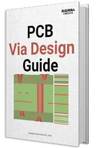
PCB Via Design Guide
7 Chapters - 90 Pages - 70 Minute ReadWhat's Inside:
- Guidelines for choosing the right via for your application
- Design rules for advanced via structures
- DFM tips to avoid manufacturing errors
- Signal integrity considerations for high-speed designs
- Testing and inspection methods for via reliability
- Fab notes
Download Now
Stack-up design tips to minimize board warpage in high-power PCBs
Heavy copper weights, asymmetric stack-ups, and uneven copper distribution create differential mechanical stress across the PCB. This causes warpage that reduces assembly yield and increases solder joint stresses. Severe warpage can crack BGA and ceramic components and create intermittent electrical contact issues.

To prevent warpage:
- Balance copper weight across the high-power circuit board stack-up.
- Add copper thieving on sparse layers.
- Follow IPC-6012 bow and twist limits.
- Use high-Tg materials for elevated temperatures.
- Avoid highly asymmetric builds, especially with thick outer-layer copper.
Best practices to ensure vibration-resistant PCBs
Automotive, aerospace, and industrial electronic systems are exposed to continuous vibration and mechanical shock. Excessive vibration can damage solder joints, crack PCB traces, deform the board structure, and detach components from the assembly. Large and heavy components are especially vulnerable in high-vibration environments.
To ensure a vibration-resistant board:
- Use adhesive or underfill materials to secure large components.
- Reinforce flexible regions with PCB stiffeners where necessary.
- Secure tall or bulky components to minimize movement.
- Implement proper strain relief for cables and connectors.
- Select connectors designed for vibration-prone environments.
How to minimize connector stress on circuit boards
High-current connectors and cable assemblies apply continuous mechanical force on the PCB during installation and operation. Poor mechanical support can damage solder joints and mounting regions over time.
To reduce connector-related mechanical stress:
- Place large connectors near mounting holes to improve board stability.
- Use through-hole connectors when additional mechanical strength is required.
- Reinforce mechanically stressed regions with additional support structures (mounting brackets and metal stiffeners).
- Minimize unsupported cable loading on the printed board.
High-power PCB failures are usually preventable through efficient thermal, electrical, and mechanical design practices. Reliable layouts require accurate current calculations, controlled conductor spacing, balanced stack-ups, and robust interconnect structures.
Manufacturing constraints must also be considered early to improve yield and long-term reliability. Early thermal analysis, insulation planning, and DFM validation significantly reduce field failures and improve product lifespan.
About the technical reviewer:
Dilip Kumar is the Senior Design Manager at Sierra Circuits with over a decade of experience in developing high-speed and HDI PCB designs featuring fine-pitch BGAs. He is proficient in Altium Designer, Cadence Allegro, Eagle PCB, KiCAD, and AutoCAD.
Leading a team of skilled designers and layout engineers, he oversees projects from concept to production, ensuring precision and manufacturability at every stage. Dilip consistently delivers innovative, high-quality designs that meet demanding engineering and business objectives.
Have questions about designing high-power PCBs? Post them on SierraConnect. Our PCB experts will help you.

About Mohamed Faheemuddin : Mohamed Faheemuddin is a mechanical engineer. His passion for electronics drew him to the PCB industry. With an experience of over 3 years in the PCB industry, he specializes in developing articles for engineers and hardware designers.


Start the discussion at sierraconnect.protoexpress.com