


Contents

On-demand webinar
How Good is My Shield? An Introduction to Transfer Impedance and Shielding Effectiveness
by Karen Burnham
Standards such as IPC-2221, IPC-2152, and IPC-6012 help PCB designers select the right materials, build layouts with sufficient clearances, and meet the manufacturability requirements.
PCB designers and hardware engineers should be aware of these benchmarks to avoid expensive redesigns, ensure compliance with industry requirements, and reduce time-to-market.
In this article, you’ll learn the key IPC standards that define critical PCB design and manufacturing aspects, including material selection, layout design, and assembly quality.
Watch the full webinar here: Key IPC standards every PCB designer should know.
Highlights:
- Follow IPC-2221 and IPC-2152 to define conductor spacing, trace widths, thermal management requirements, and current-carrying capacity.
- Select rigid, flex, and high-speed laminate materials using IPC-4101, IPC-4202, and IPC-4103 specifications.
- Choose the appropriate IPC-6012 class to meet product reliability, inspection, and performance requirements.
- Improve assembly quality and manufacturing yield using IPC-7351, IPC-A-610, and J-STD-001 requirements.
Why PCB designers should follow IPC standards

Sticking to the industry benchmarks helps ensure consistent quality, reliability, and manufacturability throughout the circuit board development process. They establish globally accepted guidelines for the entire product lifecycle.
By following IPC specifications, designers can:
- Specify minimum requirements for trace widths, clearances, and material properties to withstand thermal and mechanical stress.
- Improve communication among designers, manufacturers, and assemblers.
- Facilitate compliance with regulations such as RoHS, REACH, and UL.
Ignoring them can lead to:
- Reliability issues such as overheating, shorts, and weak solder joints.
- Increased defects, rework, and fabrication or assembly delays.
The infographic below highlights common design issues caused by misinterpreting IPC requirements.

Note: IPC is now officially known as the Global Electronics Association. However, existing IPC standard designations (such as IPC-6012) and certifications remain unchanged.
Important IPC standards every PCB designer should know
The table below summarizes the key IPC specifications discussed in this article, along with their purpose and typical applications.
| IPC standard | Purpose | When to use it |
|---|---|---|
| IPC-D-356 | PCB connectivity verification | Validate netlists and support bare-board electrical testing |
| IPC-2581 | Design data exchange | Transfer PCB design, fabrication, and assembly data in a single file |
| IPC-4101 | Rigid PCB material specifications | Select laminates for rigid and multilayer boards |
| IPC-4202 | Flex PCB material specifications | Select dielectric materials for flexible circuits |
| IPC-4103 | High-speed laminate requirements | Choose materials for high-frequency and high-speed designs |
| IPC-2221 | Generic PCB design rules | Define clearances, creepage distances, and layout requirements |
| IPC-2152 | Current-carrying capacity estimation | Determine trace widths based on current and temperature rise |
| IPC-6012 | PCB performance classification | Select the appropriate reliability class for your application |
| IPC-7351 | Land pattern design | Create standardized component footprints |
| IPC-A-610 | Assembly acceptability criteria | Inspect and evaluate assembled PCBs |
| IPC J-STD-001 | Soldering requirements | Manufacture reliable soldered electronic assemblies |
Let’s see each of these in detail:
1. IPC-D-356: Electrical connectivity verification and netlist validation

IPC-D-356 provides a standardized netlist format that verifies electrical connectivity before assembly. It serves as a reference for manufacturers to confirm that the fabricated board matches the intended design and helps identify connectivity issues early in the production process.
It helps you identify:
- Missing connections between nets.
- Unintended shorts caused during fabrication.
- Misrouted or incorrectly assigned nets.
Additionally, it supports bare-board electrical inspection, such as flying probe testing.
Best practices for creating an accurate IPC-D-356 netlist:
- Include the netlist file with the fabrication drawing.
- Ensure the netlist is labeled with the correct part number and design revision.
- Specify any intentional electrical shorts in the netlist to prevent manufacturing delays.
Note: Include an IPC-D-356 netlist when submitting the design data through Gerber files. For ODB++ and IPC-2581, a separate netlist file is not required because it is embedded in these file formats.
2. IPC-2581: Standardized design data for PCB manufacturing

IPC-2581 combines circuit board design, fabrication, and assembly information into a single standardized file. It enables consistent data interpretation across different EDA tools and helps reduce translation errors during manufacturing.
IPC-2581 (IPC-DPMX) includes:
- Schematic and netlist data.
- Circuit board Stack-up and impedance specifications.
- Drilling, routing, and plating information.
- Dielectric, inner, and outer copper layer information.
- Bill of materials (BOM).
- Solder mask and paste layer data.
- Component and footprint information.
- Board features such as blind vias, buried vias, slots, V-grooves, and cavities.
While on the subject, we got one question from a designer saying, “Are fabrication and assembly drawings still required when submitting a PCB package? If so, what standards should be referenced, and what design and fabrication specifications should be included?”
Gopal, Director of CAM at Sierra Circuits, explained, “Yes, we prefer including fabrication and assembly drawings in the PCB package. Even when complete design data is provided through IPC-2581, fabrication drawings should clearly define materials, stack-up requirements, surface finishes, and any special manufacturing instructions. Similarly, assembly drawings should specify component placement, orientation, and assembly notes to ensure accurate board population.”
3. IPC-4101: Material specifications for rigid and multilayer circuit boards
It defines the requirements for base materials used in rigid and multilayer boards. It specifies key material properties that influence thermal, electrical, and mechanical performance.
The standard covers parameters such as glass transition temperature (Tg), dielectric constant (Dk), and dissipation factor (Df), which help designers evaluate material suitability for different applications.
IPC-4101 also categorizes materials using slash sheets, making it easier to identify laminates based on their performance characteristics.
Filler: Filler is an additive incorporated into laminate materials to enhance thermal, electrical, and mechanical performance. IPC-4101 slash sheets classify materials based on whether they contain inorganic fillers or no fillers.
| Slashsheet | Material type | Filler type |
|---|---|---|
| IPC-4101/99 | Epoxy-based materials with a minimum Tg of 150°C and Td of 325°C | Inorganic |
| IPC-4101/124 | Epoxy-based materials with a minimum Tg of 150°C and Td of 325°C | NA |
| IPC-4101/101 | Difunctional epoxy-based materials with a minimum Tg of 110°C and Td of 310°C | Inorganic |
| IPC-4101/121 | Difunctional epoxy-based materials with a minimum Tg of 110°C and Td of 310°C | NA |
| IPC-4101/126 | High-performance epoxy-based materials with a minimum Tg of 170°C and Td of 340°C | Inorganic |
| IPC-4101/129 | High-performance epoxy-based materials with a minimum Tg of 170°C and Td of 340°C | NA |
IPC-4101 helps you evaluate:
- Material suitability for high-speed designs
- Thermal stability for demanding environments
- Electrical and mechanical performance
For more, download the IPC Standards Handbook.
IPC Standards Handbook
7 Chapters - 110 Pages - 85 Minute ReadWhat's Inside:
- Clear breakdown of IPC standards for every stage of PCB development
- Design and DFM guidelines based on IPC-2221, IPC-7351, and IPC-J-STD-001
- Material selection guidance tied to IPC-4101, IPC-4202, and more
- Testing and inspection insights using IPC-A-600 and IPC-TM-650
- Best design documentation practices for seamless production
Download Now
4. IPC-4202: Requirements for flex dielectric materials
It defines the requirements for flex dielectric materials used in flexible PCBs. IPC-4202 uses slash sheet codes to classify quality-assured laminates based on their dielectric type, reinforcement, and thickness.
| Designation | Material type | Reinforcement | Typical use |
|---|---|---|---|
| IPC-4202/1-E1E2 | Polyimide (E) | Non-reinforced film (1) | Thin polyimide for single/double-layer flex |
| IPC-4202/2-E3E3 | Polyimide | Woven reinforcement film (3) | Reinforced polyimide for increased strength |
| IPC-4202/3-A1A2 | Polyvinyl fluoride (PVF, A) | Non-reinforced film (1) | Low-cost flexible dielectric |
| IPC-4202/4-C1C2 | FEP fluoropolymer (C) | Non-reinforced film (1) | High-temperature applications |
| IPC-4202/5-D3D4 | PTFE (D) | Woven reinforcement (1) | Ultra-low loss for RF/microwave flex |
How to interpret slash codes:
Let’s understand how to read an IPC-4202 slash code with an example.
Slash sheet code format: IPC-4202/<sheet>-<Dielectric><Reinforcement><Thickness>
Where:
- Dielectric type is represented by alphabets (Eg: A = PVF, E = polyimide, C = FEP, and D = PTFE)
- Reinforcement is represented by numbers (Eg, 1 = non-reinforced
- and 3 = woven)
- Thickness is represented by the last part (Eg, E2 for the thickness of 50 µm)
Here’s a prompt that can help you select the right IPC-4202 slash sheet using a generative AI tool:
Act as a PCB materials expert and recommend the most suitable IPC4202 slash sheet code based on the following requirements:
- Application: [e.g., medical wearable, aerospace]
- Material: [e.g., Polyimide, Polyester]
- Reinforcement: [Non-reinforced/woven-E-glass]
- Construction: [Adhesiveless / adhesive-based]
- Thickness: [e.g., 50 µm]
- Key needs: [e.g., High-frequency low loss, UL 94V-0, tight bend radius]
For rigid-flex PCBs, IPC-2223 provides design guidelines, and IPC-6013 specifies the qualification and performance requirements.
Need help in designing your circuit boards? Check out Sierra Circuits’ PCB design support. Our engineering team can help you with stack-up, layout, and DFM analysis.

5. IPC-4103: Performance specifications for high-speed laminates

This document covers material characteristics such as signal loss across different frequency ranges.
IPC-4103-qualified laminates, such as Rogers RO4350B and Isola Tachyon 100G, exhibit minimal dielectric constant variation, typically within ±0.05 over 1 to 20 GHz.
The standard also covers bonding, clad, and unclad plastic materials used in high-speed circuits.

6. IPC-2221: Fundamental PCB design requirements and layout guidelines

IPC-2221 defines the fundamental design requirements for printed circuit boards. It provides guidance on material selection, electrical properties, thermal management, physical board characteristics, interconnections, and documentation requirements.
IPC-2221B defines minimum creepage and clearance distances to help prevent electrical failures in printed boards.

| Feature | Clearance |
|---|---|
| Component leads | 0.13 mm (up to a voltage of 50 V) |
| Uncoated conducting areas | 0.75 mm |
| Test probe sites | 80% of the component height (0.6 mm minimum and 5 mm maximum) |
| Mounting hardware | Should not protrude more than 6.4 mm below the PCB surface |
| PTH relief in the heat sink | 2.5 mm larger than the hole (includes electrical clearance + misregistration tolerance) |
How to calculate trace current capacity using IPC-2221

IPC-2221 provides an empirical formula to estimate PCB trace current capacity based on allowable temperature rise, copper thickness, and trace cross-sectional area.
The general equation is I = k × ΔT^0.44 × A^0.725
Where:
- I = current (A)
- ΔT = temperature rise (°C)
- A = cross-sectional area (mil²)
- k = constant (0.024 for internal layers and 0.048 for external layers)
The trace cross-sectional area (A) is calculated as: A = trace width × copper thickness
IPC-2221 Appendix A defines three circuit board test coupon types: A/B, D, and impedance. They are used for microsection analysis and evaluating interconnect reliability under thermal stress.
During the live webinar, an engineer asked, “Is IPC-2222 for PCB cross-sections?”
Gopal explained, “The IPC-2222 standard specifies the optimized rules for component placement, routing, and electrical functionality to achieve a flawless design. The document sets standards for holes and interconnections, dielectric spacing, material selection, routing parameters, board thickness tolerances, mechanical features, connector clearances, and wear structures.”
7. IPC-2152: Accurate circuit board current-carrying capacity estimation
This standard does not define a single universal formula to calculate current-carrying capacity. It is based on empirical test data and thermal measurements.
It uses charts and graphs to relate current, trace width, copper thickness, and temperature rise (ΔT).
IPC-2152 captures non-linear behavior and accounts for real-world design factors such as board thickness, adjacent copper planes, vias, and environmental conditions. dielectric thermal conductivity, copper thickness, and overall board construction.
It also provides current-versus-temperature-rise curves for both internal and external traces. The table below shows the standard line widths for different current carrying capacity.
| Current (A) | ΔT (°C) | Copper (oz/ft²) | Layer | Approx. width (mil) |
|---|---|---|---|---|
| 1 | 10 | 1 | External | 10 |
| 1 | 10 | 1 | Internal | 30 |
| 2 | 20 | 1 | External | 30 |
| 2 | 20 | 1 | Internal | 80 |
| 5 | 20 | 2 | External | 50 |
IPC-2221 and IPC-2152 are frequently compared because both benchmarks address trace current-carrying capacity and line width. The table below summarizes the differences.
IPC-2221 vs. IPC-2152
| Parameter | IPC-2221 | IPC-2152 |
|---|---|---|
| Standard type | Generic PCB design standard | Specialized standard for current-carrying capacity |
| Method | Single empirical formula | Data-driven charts and graphs |
| Accuracy | Approximate | More accurate and realistic |
| Key factors | Trace area and temperature rise | Copper thickness, layer position, planes, vias, and environment |
| Thermal modeling | Simplified | Detailed and specific to the context |
| Internal and external trace width estimation | Fixed assumptions | More refined and realistic behavior |
| Design flexibility | Limited | High (supports optimization) |
| Ease of use | Simple and quick calculations | Requires charts, tools, or calculators |
| Relevance | Baseline reference | Recommended for modern PCB design |
| Typical outcome | Overestimated trace width | Optimized (often smaller but safe widths) |
Another design engineer enquired during the live webinar, saying, “What is the limiting factor for internal trace temperature rises?”
Pranav, Team Lead, Engineering Tools R&D at Sierra Circuits, answered, “The temperature rise of internal traces depends on the dielectric’s thermal conductivity, copper thickness, and the overall board construction. According to IPC-2152, internal and external traces with similar configurations exhibit nearly the same temperature rise, as shown in the standard’s reference charts.”
8. IPC-6012: Choosing the right circuit board class for your product
IPC-6012 outlines performance requirements across four end-product classes, each representing a different level of reliability and quality.
During a survey of PCB designers, we asked which certifications they generally consider when selecting a PCB manufacturer. The results are shown below:
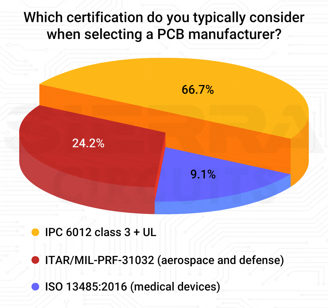
- 66.7% of respondents selected IPC-6012 class 3 and UL certifications.
- 24.2% voted for ITAR/MIL-PRF-31032 for aerospace and defense applications.
- 9.1% selected ISO 13485:2016 for medical device applications.
The table below summarizes the characteristics, design, and manufacturing considerations for each IPC-6012 class.
| Class | Name | Characteristics | Design and manufacturing considerations |
|---|---|---|---|
| Class 1 | General electronic products |
|
|
| Class 2 | Dedicated service for electronic products |
|
|
| Class 3 | High-reliability electronic products |
|
|
| IPC-6012 FS | Space, military, and avionics |
|
|
Sierra Circuits manufactures and assembles reliable IPC 6012 class 3/FS circuit boards.
To learn more, visit aerospace & defense PCB manufacturing and assembly capabilities.
To talk to a PCB expert: Book a meeting or call us at +1 (800) 763-7503.
5 important conditions specified in IPC 6012 are:
- Voids: Class 2 allows one void in 5% of the holes. Class 3 allows no voids.
- Copper plating thickness: The plating thickness requirement for class 2 is 0.8 mil and 1 mil for class 3.
-
IPC-6012F allows you to specify copper thickness in microns, and this is often considered a preferred unit in the standard. However, in industry practice, copper thickness is still widely expressed in ounces per square foot.
-
- Annular ring: Class 2 may allow up to a 90° breakout in isolated instances.
For class 3, the minimum internal annular ring is 1 mil, and the external annular ring is a minimum of 2 mil. Class 3 generally does not permit any breakout. - Dielectric thickness: Class 3 PCBs must maintain a minimum dielectric spacing of 2.56 mil between conductive layers.

An illustration that shows barrel fill requirements for IPC class 2 and class 3 boards. - Barrel fill: According to the IPC-A-610 revision H, the acceptable conditions for barrel fill are specified in the table below:
| IPC class | Minimum barrel fill | Conditions |
|---|---|---|
| Class 2 | 75% or 50% if the exception applies | Exceptions:
|
| Class 3 | 75% with no exception |
|
We received a query from a designer saying, “How can we define the edge board plating?”
Gopal explained, “Edge board plating can be defined based on the specific application and requirements.
For edge connectors, commonly known as gold fingers, hard gold plating is typically used. This involves nickel plating over copper, followed by a layer of hard gold to ensure durability and good electrical contact.
If you are referring to plating along the board edges (peripheral edge plating), this can be applied selectively to specific areas or across the entire board perimeter, depending on your design needs. However, it is important to leave some unplated areas or tooling rails to allow proper handling of the PCB during manufacturing.”
To learn how to design PCBs for harsh environments, download the IPC Class 3 Design Guide.

IPC Class 3 Design Guide
8 Chapters - 23 Pages - 35 Minute ReadWhat's Inside:
- IPC guidelines for manufacturing defects
- IPC standards for assembly processes
- Common differences between the classes
- IPC documents to set the level of acceptance criteria
Download Now
9. IPC-7351: Standardized land pattern and footprint design
The standard provides a formula for calculating land pattern dimensions:
Pad size = Component dimension + tolerance adjustments + solder fillet goal + fabrication allowance
IPC-7351 defines three standard density levels:
- Level A: maximum land protrusion with the least density
- Level B: nominal land protrusion with medium density
- Level C: minimum land protrusion with the highest density
Level A has the largest courtyard excess, while Level C has the smallest.

To standardize CAD library footprints, IPC-7351 promotes a zero component orientation convention:
- Pin 1 in the upper left quadrant: For components like IC chips, capacitors/resistors/inductors, SOICs, QFPs, diodes, and LEDs.
- Pin 1 in the lower left quadrant: For components with molded body (tantalum caps) and metal electrode face (MELF).
IPC-7351 focuses on footprint design for SMDs. IPC-7352 provides land pattern guidelines for both surface-mount and through-hole components.
Designs with a large number of through-hole components typically result in longer assembly lead times and higher labor costs, as they often require manual or selective soldering processes. They can also be less scalable for high-volume production.
In contrast, SMT designs generally enable faster production, lower costs at scale, and improved manufacturability due to their compatibility with automated assembly processes.
10. IPC-A-610: Acceptability criteria for electronic assemblies
IPC-A-610 defines how to determine whether an assembly is acceptable or defective through visual inspection.
This standard covers:
- ESD protection circuits.
- Mounting hardware, such as fasteners (screws, nuts, and washers) and securing hardware (clips and clamps).
- Connector installation, such as edge connectors, press-fit pins, and heatsinks.

- Solder joint defects, such as solder bridges.
- Parts that get damaged during assembly, such as chips or cracks.
- Base material conditions like blistering, delamination, weave exposure, and board damage (scratches, dents).
- Conformal coatings, including coverage, thickness, bubbles, and adhesion, as well as encapsulated components.
11. IPC J-STD-001: Requirements for soldered electronic assemblies

IPC J-STD-001 specifies the criteria for producing reliable soldered electronic assemblies.
This standard covers:
- Solder alloys, including traditional tin-lead (e.g., Sn63Pb37, Sn62Pb36Ag2) and various lead-free alloys (e.g., SAC alloys like Sn96.3Ag3.7).
- Soldering principles such as wetting, solder flow, and thermal profiles.
- Solder paste application, component placement accuracy, and reflow soldering profiles.
- Specific criteria for different SMT component types, such as chip components, gull-wing leads, BGAs, and QFNs.
- Process control methods for classes 2 and 3.
- Manufacturing environment requirements, including temperature (18 – 30°C), humidity (30 – 70% RH), lighting (>1000 lux), and ESD protection as specified by ANSI/ESD S20.20 or IEC 61340-5-1.
- Use of X-ray inspection for evaluating certain solder conditions, particularly for PTHs.
IPC guidelines help designers build reliable and compliant circuit boards. By following standards such as IPC-2221, IPC-2152, IPC-6012, and IPC-A-610, designers can improve product quality, reduce expensive redesigns, and streamline manufacturing.
About the technical reviewer:
Gopal is an accomplished DFM/CAM engineer with over 30 years of experience in optimizing PCB manufacturing processes. At Sierra Circuits, he guides the planning and CAM teams to achieve the desired results. Gopal’s expertise in DFM guidelines and fabrication techniques enables him to build error-free circuit boards.
Not sure which IPC standards apply to your design? Post your questions on our PCB forum, SierraConnect. Our design and manufacturing experts can help you choose the right class, materials, and design requirements.


Start the discussion at sierraconnect.protoexpress.com