Contents
PCB outgassing or offgassing is a defect that occurs when air is trapped inside a circuit board during production. The trapped air creates voids or blowholes, which might damage the board’s performance. Choosing a low outgassing rate material and vacuum pre-baking are some well-known methods to reduce the adverse effect of outgassing in circuit boards.
What is outgassing in PCBs?
Outgassing is a defect that occurs when trapped gas/vapor is released from the printed circuit board when exposed to heat or vacuum, creating blowholes, lamination voids, and plating voids. Offgassing affects a wide range of electronic applications that are used in high-vacuum conditions such as satellites, space-based equipment, and medical devices. Low outgassing board materials are the right choice for these kinds of applications.
Mechanisms contributing to outgassing

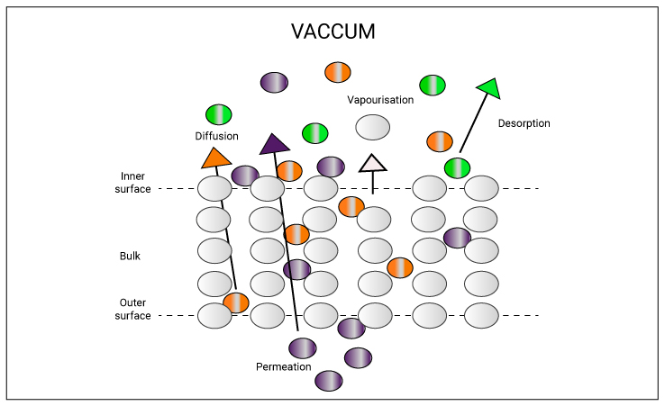
Outgassing is caused by four different mechanisms.
- Vapourisation — Release of molecules from the material’s surface.
- Desorption — Release of molecules trapped at an internal fixture.
- Diffusion — Flow of molecules from a material’s interior structure to its outer surface.
- Permeation — Flow of molecules from the external environment to the vacuum surface through the material.
When does outgassing occur in a PCB?
Outgassing occurs during the soldering process and can also occur when the board is exposed to high temperature and vacuum conditions. Poor material choices and manufacturing errors also cause it.

Outgassing during the soldering process
When a circuit board is soldered, any moisture present near the hole is heated and converted to vapor. This gas causes gaps in the solder mask when it escapes. Outgassing can occur due to the following:
- Presence of moisture in the circuit board: Moisture removal from the PCB is vital. To achieve this, boards should be baked. Baking is the process of eliminating volatile molecules from circuit board materials by heating them to a high temperature (100 to 125°C). IPC-1601 describes the standard for circuit board baking to eliminate outgassing. This procedure should be carried out in a clean oven to protect the board from any contamination that may occur during the process. It’s also a good option to place the PCBs in such a way that air can readily move around them throughout the baking process. To know how contamination leads to board failure, read why we perform PCB ionic contamination analysis?
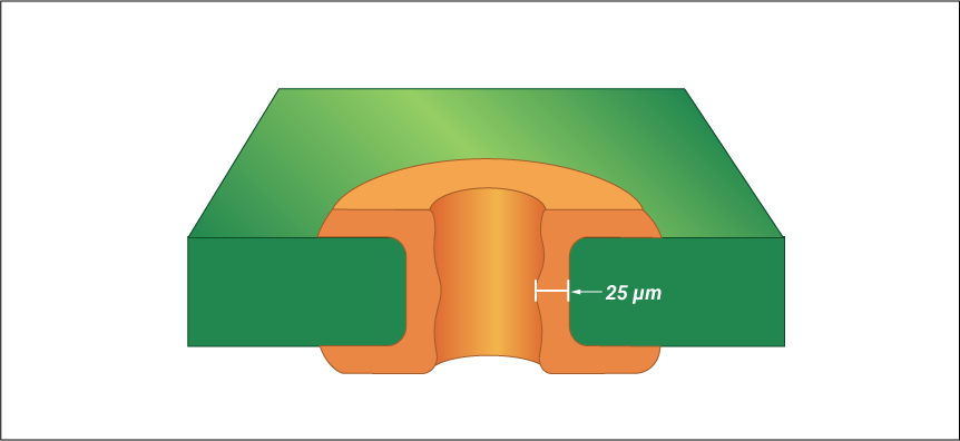
- Thin through-hole plating (less than 20µm): Air can come through the plated hole wall if the coating is thin or if there are voids in the copper plating. To avoid this, hole plating thickness should be at least 25µm.
Also read, 8 soldering tips to watch out for.
Exposure to an ultra-high vacuum environment
Circuit boards that are implemented in space and military applications operate under ultra-high vacuum (UHV) environments. Dielectric materials will lose their mass when exposed to the UHV environment. The materials start evaporating and the adsorbed material on the circuit board surface will start desorbing (releasing gas). This results in outgassing. The expelled vapor can condense on optical devices such as cameras and can affect their image-capturing quality.
Use of inappropriate material
Board materials and component packages should be selected based on their mechanical and thermal abilities as they impact the lifecycle of the PCB. To avoid offgassing, designers need to ensure that the materials have low outgassing rates and can withstand fluctuating pressure and temperature. PCB materials such as Rogers’ RT/duroid series and Nelco’s meteorwave series have low offgassing rates. These materials are thermally stable and impose outstanding resistance to this defect.
What is considered as a low outgassing rate?
A board material with collected volatile of less than 0.1% and total mass loss of less than 1% when placed in a vacuum for 24 hours at a temperature of 125°C is considered as the substrate with low outgassing rate. Below table lists a few dielectric materials with low offgassing rates.
| Manufacturer | Material name | Outgassing data | |
|---|---|---|---|
| Total mass loss % (max 1%) | Collected volatiles % (max 0.1%) |
||
| Rogers Corporation | RT/duroid 5870 | 0.02 | <0.01 |
| Rogers Corporation | RT/duroid 5880 | 0.01 | <0.01 |
| Rogers Corporation | RT/duroid 5880LZ | 0.01 | 0.01 |
| Rogers Corporation | RT/duroid 6002 | 0.03 | <0.01 |
| Rogers Corporation | RT/duroid 6006 | 0.01 | <0.01 |
| Nelco | N4000-6 / 6FC | 0.27 | 0.06 |
| Nelco | N4000-7 | 0.28 | 0 |
| Nelco | N4000-13 / 13SI | 0.37 | 0.01 |
| Nelco | N4000-13EP / EPSI | 0.14 | 0.01 |
| Nelco | N4000-29 | 0.10 | 0.01 |

PCB Material Design Guide
9 Chapters - 30 Pages - 40 Minute ReadWhat's Inside:
- Basic properties of the dielectric material to be considered
- Signal loss in PCB substrates
- Copper foil selection
- Key considerations for choosing PCB materials
Download Now
How is the outgassing rate calculated?
The outgassing rate is expressed in the quantity of gas per unit surface area per unit time (pressure x volume). Torr-Liters/cm2-s and Atm-cm3/cm2-s are common units of offgassing. Outgassing rate measurements may be necessary to verify or validate bakeout techniques or surface treatments and compare different circuit board materials.
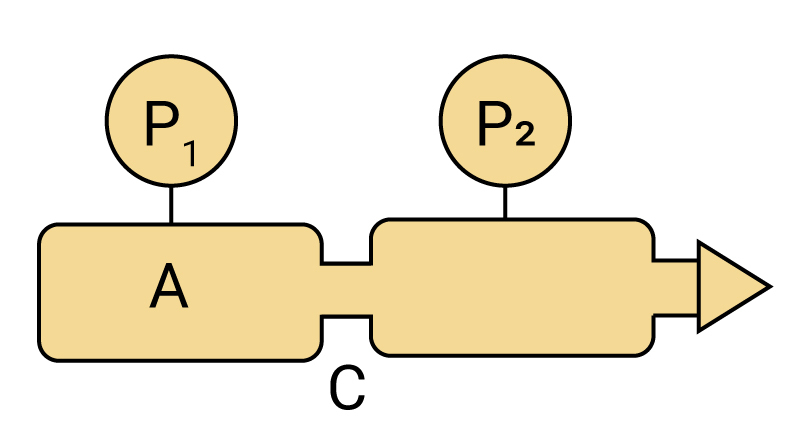
It can be measured using the conductance method. Here, the board material sample is placed in a chamber of known outgassing rate. A pump is connected to the vessel under examination and it is separated by a specific conductance. The outgassing rate is calculated by measuring the pressure decrease across the conductance.
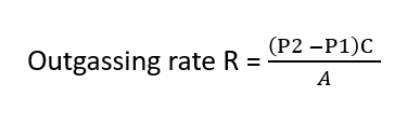
Where,
- P1 and P2 are pressure of the pumps
- C is the conductance
- A is the internal surface area of the chamber to be tested
Material evaluation check for PCB outgassing
Outgassing affects the performance of the boards that are implemented in space applications. To reduce the adverse effects due to this, NASA has designed stringent procedures to test their circuit board laminates.
SP-R-0022A
SP-R-0022A standard establishes outgassing requirements and test guidelines for circuit board materials used in space environments. This test is carried out to ensure that the materials used in space applications do not affect the sensitive surfaces of any adjacent equipment.
ASTM E595-07
American society for testing and materials (ASTM) has also designed a test procedure to assess PCB materials. This test evaluates material properties such as TML (total mass loss) and CVCM (collected volatile condensable material).
Test procedure
- The test sample is placed in a vacuum environment for 24 hours at a temperature of 125°C.
- The sample is weighed at 23°C after a 24-hour period. This reduces the impact of water vapor on the measurement. Then the sample is constantly weighed over a 2-minute period to reduce water vapor absorption loss since it is exposed to an uncontrolled environment.
Criteria of acceptability
The board material shall have volatile condensable content of less than 0.1% of the original mass of the sample. The total mass loss of the material shall not exceed 1% of the original mass of the sample.
How can we prevent PCB outgassing in space applications?
As mentioned earlier, outgassing is a common occurrence in ultra high-vacuum conditions and it can also hamper or destroy neighboring instruments. Designers need to figure out how to limit this defect in the boards that are implemented in UHV conditions. Offgassing can’t be eliminated completely, however, it is essential to have strategies to mitigate the occurrence of it. The following pointers can help PCB designers tackle this problem:
- Verify that the circuit board and its components can resist the extreme temperature swings in space. This is in addition to the electro-thermal modeling of PCB layouts prior to manufacture, which is required for all board designs.
- Vias can be sources of outgassing because it is associated with drilling holes. To avoid this, maintain uniform temperature dissipation and distribution throughout the PCB manufacturing and assembly processes.
- The vacuum pre-bake process should be carried out to get the moisture out of boards as much as possible.
- Ensure that the materials are specifically developed for the end application (materials made for vacuum environments), such as Rogers Corporation’s RT/duroid series. Some flexible circuit materials, such as Kapton, offer excellent outgassing properties.
- The effects of offgassing can be reduced by directing vapor away from sensitive surfaces and employing heating devices. Create a path for any released gases and direct them into space.
- Hole plating should be a minimum of 25µm.

Fab notes to avoid outgassing in PCBs
- Bake the boards at a temperature between 100 to 125 °C.
- Hole plating thickness should be at least 25µm.
- Always use thermally stable materials. Materials such as Rogers’ RT/duroid series and Nelco’s meteorwave series have low outgassing rates. Also, ensure that materials have passed outgassing evaluation tests based on the standards SP-R-0022A and ASTM E595-07.
- The board temperature should not exceed 125 degrees.
- Avoid hotspots if possible.
Outgassing has the potential to hinder the reliability of circuit boards that operate in high-temperature and high vacuum environments. Thus it is essential for the PCB designers to know about outgassing and the methods to control it. Choosing the right material for your board can make a lot of difference. Let us know in the comments section if there is anything more you want to learn concerning offgassing.

Design for Manufacturing Handbook
11 Chapters - 96 Pages - 90 Minute ReadWhat's Inside:
- Annular rings: avoid drill breakouts
- Vias: optimize your design
- Trace width and space: follow the best practices
- Solder mask and silkscreen: get the must-knows
Download Now
About Milan Yogendrappa : Milan Y is an electronics and communication engineer with over 6 years of experience in developing and editing technical articles related to PCB design, manufacturing, and assembly. He is currently the editor-in-chief at Sierra Circuits.