


Contents
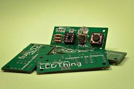
One of the major concepts in electronics is the printed circuit board or PCB. It’s so fundamental that people often forget to explain what a PCB is. Electronics have come a long way. A journey that started with vacuum tubes and relays got its way into silicon and ICs. It became more prevalent in consumer goods. Therefore, there is always pressure to reduce the size and manufacturing costs of electronic products. This drove manufacturers to look for better solutions.
Inside a PCB
Imagine a life full of wires, like loads and loads of wires.
Imagine connecting your motherboard with a bunch of wires or even your phone. Can you make an idea what size will that mobile be? Thus PCB was born to fit our delicate daily use products into their super fancy outer cases.
Here we assume you’ve likely flown in an airplane at least once in your life. My favorite part of the journey is when the plane slowly approaches higher. What’s yours?
As you approach higher you get a new perspective of your own city, which you can only get when you’re at a specific height. What do you see? A well-connected system of roads, buildings, cars, houses, and people. Same as that, circuit boards are complete systems. They provide a foundation for all of the electronic components that make our objects come to life.
Confused? Let’s first understand out of what a PCB is made.
A PCB is typically like a layer cake or lasagna. If not deliciously but delicately placed alternating layers of different materials. They are laminated together with heat and adhesive such that the result is a single object.
Let’s start in the middle and work our way out.
The base material, or substrate, is usually fiberglass. Historically, the most common designator for this fiberglass is “FR4”. Fiberglasses are stacked upon one another and are fixed with resin and made one unit that is strong enough to hold the board. There are also flex PCBs built on flexible high-temperature plastic.

Cheaper PCBs are ought to be made with other materials. Epoxies or phenolics lack the durability of FR4 but are much less expensive. These types of substrates are also found in low-end consumer electronics.
PCBs can be single-sided (one copper layer), double-sided (two copper layers on both sides of one substrate layer), or multi-layer (outer and inner layers of copper, alternating with layers of substrate).
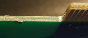
The next layer is a thin copper foil. It is laminated to the board with heat and adhesive. Generally, on double-sided PCBs, copper is applied to both sides of the substrate. In less expensive electronic gadgets the PCB may have copper on only one side. When we say double-sided or 2-layer board, we are referring to the number of copper layers in our lasagna.
This lasagna can be as few as 1 layer or as many as 16 layers or more.
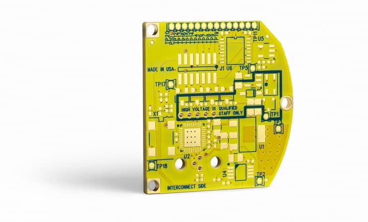
The layer on top of the copper foil is termed as the solder mask layer. This layer gives the PCB its typical green color. It is applied onto the copper layer to insulate the copper traces. It nullifies the chance of accidental contact with other metal, solder, or conductive bits. This layer helps the user to solder to the precise places and prevent solder jumpers.
A white silkscreen layer is applied on top of the solder mask layer. This silkscreen adds letters, numbers, and symbols to the PCB. This allows for easier PCB assembly and indicators for humans to better understand the board. We often use silkscreen labels to indicate what the function of each pin or LED is.
Now coming back to our analogy:
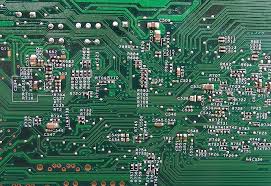
On top of a PCB, you can notice a bunch of lines running throughout the place, connecting various components. Don’t our roads do the same as well, run all over the city connecting all the places? But here instead of cars zooming around, electrons are flying down roads made out of copper, hurrying off to power one component after another! These copper roads are called traces in our PCB city.
A city is where all the major works happen. We have offices, local business etc. on every corner. This central hub of human activity is just like those square black shapes that you’ll find on a PCB called integrated circuits (ICs). These ICs are where all of the tough work happens in a PCB, doing rapid-fire calculations.
The suburbs are where homes, parks, and schools are a typical sight. From a plane, you’d notice that the rows of houses in a suburb often look just like the small resistors found all over a PCB. These resistors are out there to significantly control the flow of charge by resisting it.
No city is free from construction! Whether it’s building a new skyscraper or a new apartment complex, you’d find new foundations being laid everywhere. These foundations are just like the empty pads that you’d find on a PCB with no components on it. While they might be empty now, a component may soon be soldered to them.
Even our PCB city has its own street names and addresses.
This addressing, called silkscreen, helps people that are assembling or fixing PCBs to know exactly what a part is and where it is.
All of that corporation water we use comes from a local storage tank, and the water finds itself traveling to different places through pipes. That system is just like the holes you might find on a PCB called vias. This helps deliver electricity from one side of a PCB to another, just like how our water travels from the local storage tank to our bathroom, it’s an expressway.

Power plants in a city keep our lights running. Could you imagine what a city would be like without them? Hopefully, not zombie-infested! Just like power plants in a city, we have what we call capacitors on a PCB that store electricity. They hold up the charge and release it when it’s needed to send power.
Street lights and signs help to keep order in this world full of crazy drivers. They control the flow of traffic in our maze of streets and highways. On a PCB, the diodes and their cousins LEDs are those signs and streetlights. The diode controls the flow of electricity on a PCB. It allows it to go only in one direction.

The PCB is the foundation of our future.
It is allowing us to create, discover and improve the human experience in ways we might have never thought were really possible. But today, we’re just at the beginning of our journey with PCBs. However, we already have evolved in a way which is kind of unimaginable until recently. Maybe in the future, we might find ourselves using biodegradable circuit boards. And even call them the “Green Boards”. Or perhaps you’ll be able to 3D print your own PCB at your home!
There are so many uses to PCBs, and it all starts with you. Your bright engineering mind probably has some great ideas up there it needs to get them out. PCBs are a vast topic that requires a lot of study time and dedication. If you’re up for it, go ahead, make a change, make life a little more sleek and beautiful.
Quote and order your circuit boards online with our Turnkey PRO tools in just a few minutes.


