PCB Layout Guidelines and Grounding Techniques to Avoid EMI and Crosstalk

Amit Bahl
CRO
Sierra Circuits
Fill out the form:
How to avoid EMI and crosstalk in your PCB layout
EMI is undesired interaction between electronic circuits due to radiated and conducted electromagnetic emission. Crosstalk involves unwanted electromagnetic coupling between closely spaced traces. These factors lead to false triggering of logic functions, incorrect signal transitions, and premature component failure in high-speed PCBs.
You’ll learn some of the important design methods to effectively manage EMI and crosstalk in your designs.
Inaccurate stack-up design, grounding, propagation delay, via stubs, and impedance discontinuity are key contributors to EM emissions and crosstalk. You need to place ground planes right below the signal layer to achieve tight coupling and a shortened return path. In addition, you should avoid placing adjacent signal layers.
To help you design an error-free stack-up in a go, our experts will provide a live demo of an advanced design tool, PCB Stackup Designer.
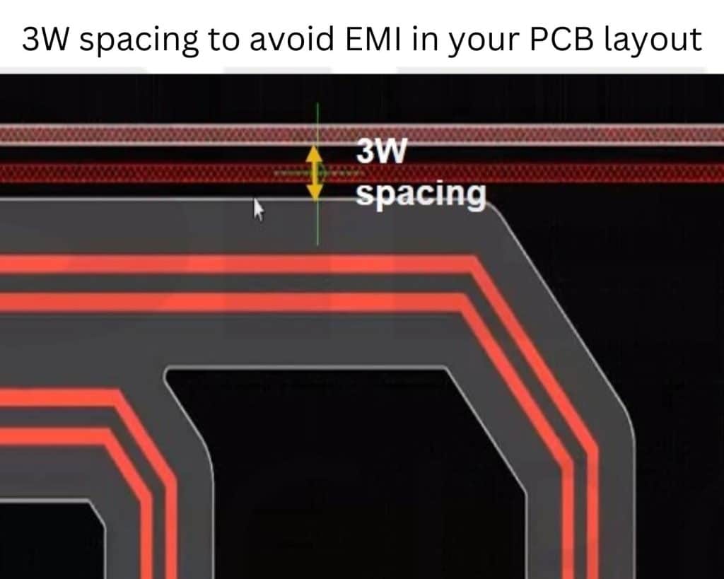
When it comes to routing, you need to ensure a 3W spacing (W represents trace width) between the conductors and position adjacent signal layers orthogonally. Differential pairs should be tightly coupled to reduce common-mode noise. Incorporate coaxial via geometry to avoid via impedance discontinuities. Decoupling capacitors and termination resistor placement also help reduce EMI, near-end (NE) and far-end (FE) crosstalks.
We will take you through the process of estimating NE and FE crosstalk in your circuit board using our cutting-edge design tool, Impedance Calculator.
A solid reference plane is crucial to achieve effective grounding. It absorbs the fringe electric and magnetic fields and prevent them from spreading to the neighboring circuits. Via stitching and star grounding facilitate a low-inductance ground plane reducing interference.
In this webinar, our design experts will take you through the best techniques to avoid EMI.
What you’ll learn:
- How to implement 3W trace clearance, via stitching, EMI shielding, and guard traces in Altium Designer
- How EMI and crosstalk impact your PCB design
- Managing near-end and far-end crosstalk
- PCB stack-up design considerations to avoid signal interference
- Layout guidelines to combat EM radiation and unwanted EM coupling
- 4 best grounding strategies
- PCB design tool demos:
Presented by Amit Bahl
Amit has been in the PCB industry for 20+ years. He is the Chief Revenue Officer at Sierra Circuits. His passion is to empower tech companies to achieve their visions and change the world. Rockets going into space, self-driving cars taking up the streets, cancer-fighting medical devices, protecting the country, he’s ready to build any circuit board!
Watch the Trailer


