Contents

On-demand webinar
How Good is My Shield? An Introduction to Transfer Impedance and Shielding Effectiveness
by Karen Burnham
Rigid-flex circuit boards are the best solution for space-constrained environments. They can withstand a significant number of flex cycles and are prominently found in satellites and aerospace and medtech applications. You must adhere to the IPC-2223 standards for rigid-flex design to avoid design violations.
IPC constantly develops standards for PCB design, fabrication, assembly, and testing. Following the IPC guidelines during the design phase will help you produce an efficient rigid-flex prototype. Over the years, IPC has established various standards to ensure design reliability and cost-effective products.
In this article, you will learn the IPC design standards to avert rigid-flex design violations.
Benefits of following IPC-2223 and other standards in rigid-flex
- From design to the production process, you will encounter the same terminologies that fall under the IPC standards. This enables you to easily communicate your requirements to your fabricator.
- Reduces the board size
- Optimizes the bending performance of the circuit
- Delays and reworks can be eliminated
- Helps in developing high-quality products

IPC-2223 and additional design standards for rigid-flex PCBs
For a more viable and efficient design, refer to the rigid and flex section design standards mentioned in IPC-2223, IPC-6013D, and IPC-6013C for qualification and performance specifications. These guidelines ensure the overall integrity of your board.
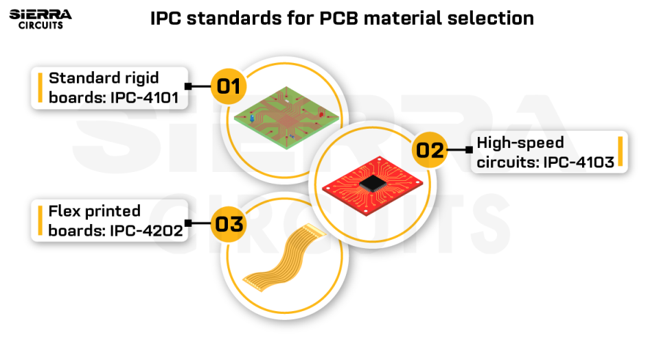
IPC-2223
- Defines the design standards for flex PCBs and various component mounting and interconnection systems.
- Provides instruction for applying electrical constraints, such as conductor clearance and controlled impedance to the flex and/or rigid circuit board.

Controlled Impedance Design Guide
6 Chapters - 56 Pages - 60 Minute ReadWhat's Inside:
- Understanding why controlled impedance is necessary
- Stack-up design guidelines
- How to design for impedance
- Common mistakes to avoid
Download Now
For rigid-flex designs, consider the following IPC-2223 recommended parameters:
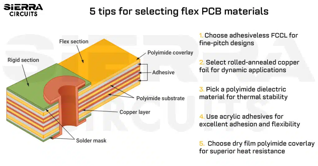
- Selection of material
- Flexibility and number of layers
- Traces width
- Impedance control
- Selective (Button) plating
- Bending radius
- Coverlay /solder mask
- Support for pads
- Copper-filled vias/microvias

IPC-6013 D
- Gives specifications for final finishes and rigid-to-flex areas.
- Provides guidelines for deformation anomalies like wrinkles, marking, annular ring, conductor thickness reductions, dielectric removal in holes, resin smear, copper-filled microvias, and selective hole plating.
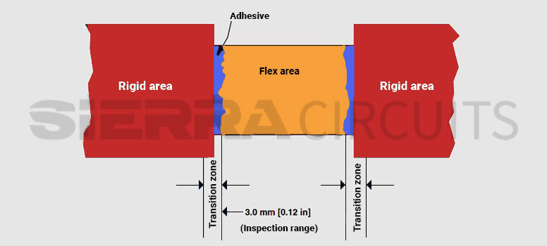
IPC-6013 C
According to IPC 6013C, the transition zone is the area centered at the rigid portion’s edge. The inspection range is limited to 3.0 mm around the center of the transition.
What are the common rigid-flex design violations?
Design violations in rigid-flex PCBs can occur in areas like flexibility, the number of layers, traces, trace geometry, drill to copper, and vias of rigid and flex areas. Avoiding common flex PCB errors will enhance the stability of your design. You can consider the guidelines as suggested below:
Flexibility and number of layers
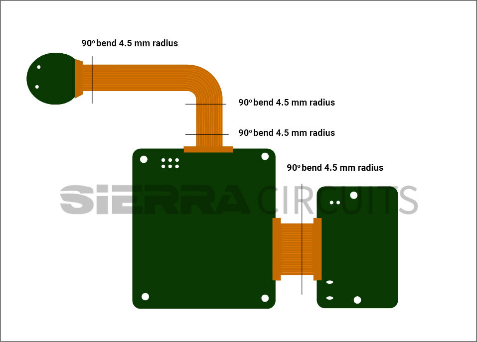
Your design must take into account how often your flexible PCB will bend. Copper will stretch and shatter if the board is bent more often than the design permits. The bend radius is the smallest angle at which the flex can bend. It can be calculated with reference to the number of layers.
| Number of layers | Bend radius (mils/mm) |
|---|---|
| 1 (single-sided) | Flex thickness x 6 |
| 2 (double-sided) | Flex thickness x 12 |
| Multi-layer | Flex thickness x 24 |
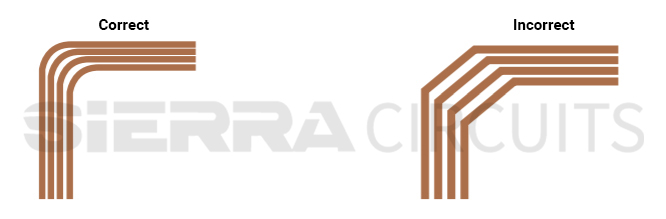
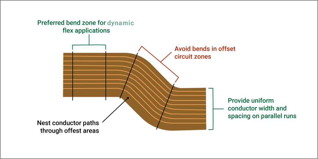
Trace routing
The circuitry’s arrangement has a direct impact on the flexibility and durability of a rigid-flex PCB. Sharp angles should never be used to route traces. This will not only make your circuit less flexible but will also put more stress on it. This will cause copper circuits to thin out at the bend radius.
In a flex PCB, a trace entering a pad creates a weak spot where the copper may eventually become worn out. It is always advised to taper the pads down near the end where they connect to the traces, as shown below.
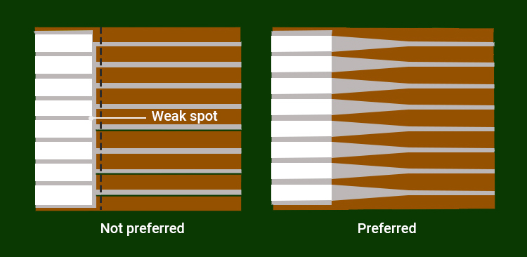
Sticking to flex PCB design guidelines for manufacturing will enhance the reliability of your design.
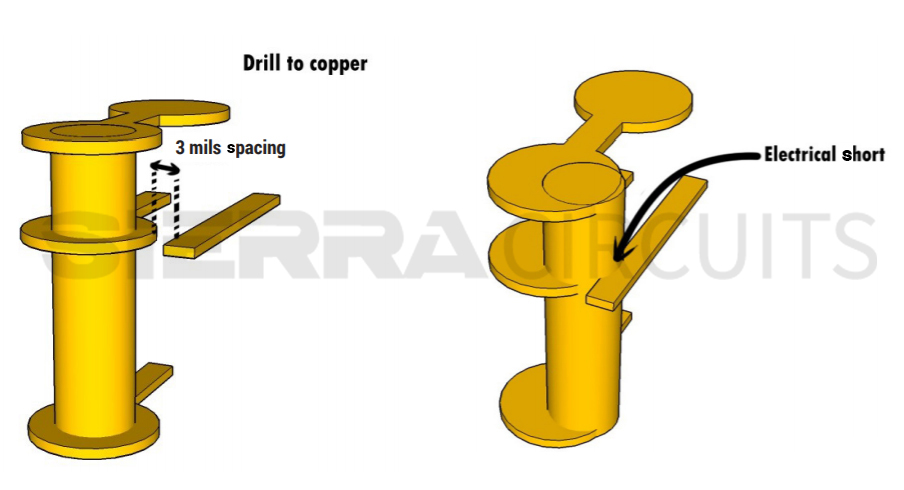
Drill-to-copper
The drill-to-copper issue must be taken into consideration while building flexible items. Drill-to-copper is required for a successful product because this material moves and shrinks during the manufacturing procedures. Drill-to-copper clearance is typically 8 mils.
Finished hole to copper clearance = drill-to-copper clearance + (plating thickness x 2)
For example, if the drill diameter is 6 mils and the plating thickness is 1 mil, the finished hole-to-copper clearance = 6 + 1 x 2 = 8 mils.
Vias in rigid and flex areas
Vias are more likely to slip away from the flex layers. To avoid misregistration, consider the following recommendations while designing:
- Avoid placing vias in areas that bend; this reduces the risk of cracking.
- Vias that are placed over a stiffener are safe, but those that are placed just off its edge are at the risk of cracking.
- The distance between vias and the rigid-flex interface should be at least 20 mils.
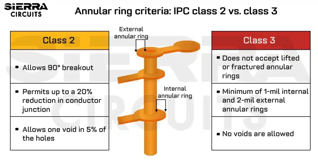
- Smaller annular rings can increase the risks associated with vias. Keep the annular rings as large as possible.
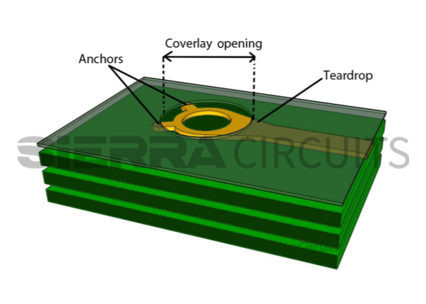
- Use teardrop-shaped vias to reduce the potential stress on the PCB. Adding tabs or anchors can also reduce peeling as depicted below.
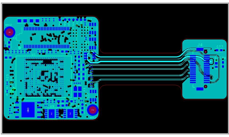
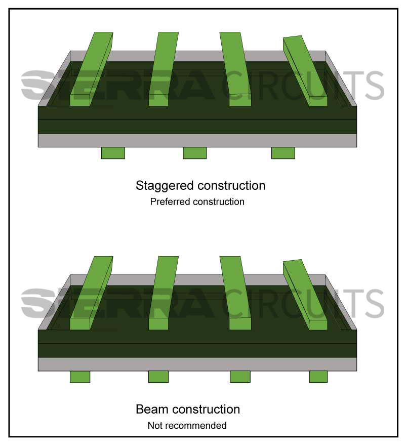
Staggered traces on different layers
Stacked traces reduce circuit flexibility and increase stress, which results in copper circuit thinning at the bend. Use staggered traces on the front and back of multilayer rigid-flex PCBs as shown below.
How to prevent design violations in rigid-flex
Stick to the recommendations given below before you start the design process.
- Implement an even number of layers. The flex layers must be placed in the middle of the stack-up.
- At least 8 mils should be drilled into the copper, as mentioned earlier.
- To enable multilayer flex to bend in a small radius without deforming, use bookbinding technique.
- Clearly define the parts that are rigid and flexible.
- If components are located in areas where the board will bend, solder joints can weaken. Consider adding stiffeners if components must be close to a flex area.
- Place components on the stiffener to prevent mechanical stress.
- Use staggered traces on the front and back of multilayer rigid-flex PCBs.
- The rigid-flex fab notes must include both rigid and flex notes separately.
- The acrylic adhesive thickness through the rigid portion of the panel should not exceed 10% of the total construction.
- Misregistration between two layers should not be greater than 0.005″.
- Surface roughness must not be more than 0.75 %.
- In the stack-up, include impedance trace details such as trace width, height, and impedance tolerance.

- Avoid using vias and pads at bends, as the mechanical stress could weaken the paddings.
- Place the traces perpendicular to the bending line for structural stability.
- To strengthen the bend area, add dummy traces to the existing traces.
- In the flex area, the ground plane should be a hatched polygon rather than solid copper planes.
- Avoid making 90-degree bends. Tighter bends cause more damage to the circuit.
- Always measure the bend radius from the inner surface.
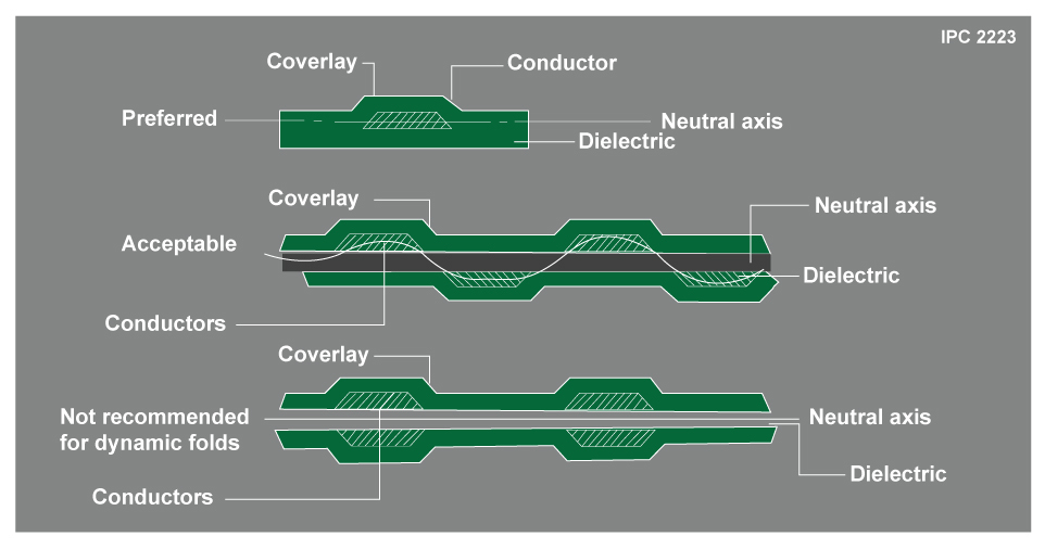
- Conductors smaller than 10 mils should be placed inside the neutral bend axis because they can withstand compression better than stretching.
- Avoid plated through-holes near the bend.
- Increase the size of the soldering surfaces and annular rings as much as possible.
- Connect traces and solder pads in a teardrop and rounded pattern.
- Make the track width and spacing as large as possible within the flexible part.
Rigid-flex capabilities at Sierra Circuits
Sierra Circuits delivers high-quality rigid-flex PCB by strictly adhering to IPC-2223 design standards. We understand the importance of these boards’ reliability and stability in modern electronic applications. Therefore, our capabilities include a detailed description of board attributes, surface finishes, laminate material, and many more. Read our case study on routing microcontroller and BGA in rigid-flex PCBs, where we efficiently routed 0.4 mm BGA and microcontroller without compromising the spacing constraints.
A few of the important design parameters are tabulated below.
| PCB attributes | Specifications |
|---|---|
| Maximum layer count | ≤ 16 |
| Minimum core thickness | 0.002″ (.051 mm) |
| Maximum finished copper thickness (O/L) | 9 micron (.009 mm) (only for O/L) |
| Smallest mechanical drill diameter | 0.0071″ (.180 mm) |
| Minimum finished hole size | 0.006″ (.152 mm) |
| Smallest laser drill diameter | 0.005″ (.127 mm) |
| Minimum trace and space | ≥ .0035”(.089 mm)(rigid) |
| Process pad diameter | D + .014″ (.356 mm) (1-mil (.025 mm) annular ring) |
| Maximum blind via aspect ratio | 0.75:1 |
Flex PCB Design Guide
10 Chapters - 39 Pages - 45 Minute ReadWhat's Inside:
- Calculating the bend radius
- Annular ring and via specifications
- Build your flex stack-up
- Controlled impedance for flex
- The fab and drawing requirements
Download Now
The main purpose of a rigid-flex circuit board is to improve the product’s integrity while saving space or assisting in the reduction of the product’s size. A well-designed rigid-flex circuit can handle a wide range of bending tasks. The important aspects of the rigid-flex design rules and possible violations have been presented here. Let us know some of the design violations that you come across in your designs in the comment section.