


Contents
PCB laminate and material selection is the first step in your PCB design process. Selecting the right materials for your design is very important as it can impact the overall performance of the board.
Before selection begins, there are many factors to be considered. Make sure material characteristics fit your specific board requirements and end application.
One of the main problems we face when manufacturing PCBs is the designers’ frequent over-reliance on the material datasheets. The data sheets provide designers with a thorough description of a material’s electrical properties. However, the data sheets fall short when taking into account various real-world manufacturing concerns, and real-world manufacturing concerns matter because they impact yield and cost.
PCB laminates and materials
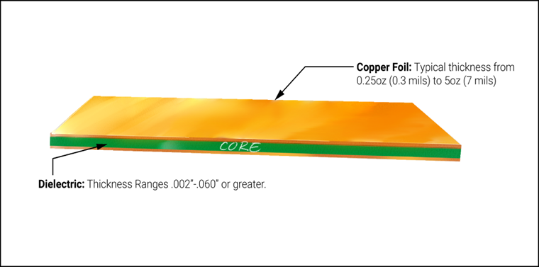
A printed circuit board is manufactured using the following 3 items:
Prepreg: B-stage material that is tacky and allows bonding of different laminates or foils.
Copper foil: Conductive traces on the PCB.
Copper-clad laminates (core): Made of prepregs and copper foils that have been laminated and cured.

Download our design guide to learn how to select the right materials for your PCBs.

PCB Material Design Guide
9 Chapters - 30 Pages - 40 Minute Read
What's Inside:
Download Now
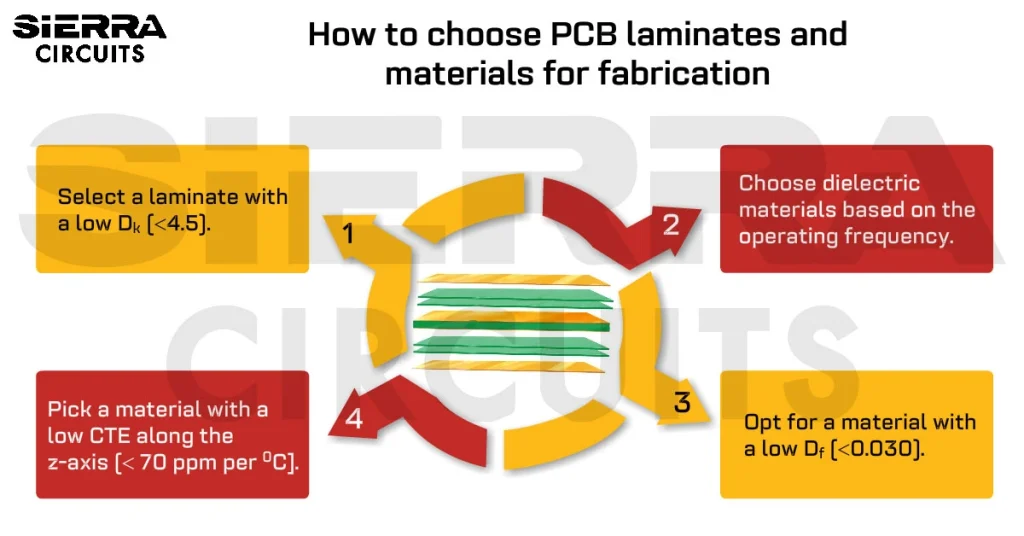
How to choose PCB laminates?
PCB laminates are made of dielectric materials. While choosing laminates, we need to consider some crucial properties of the dielectric material used. These properties include:
| Thermal properties | Electrical properties |
|---|---|
| Glass transition temperature (Tg) | Dielectric constant (Dk) |
| Decomposition temperature (Td) | Loss tangent or dissipation factor (Tan δ or Df) |
| Thermal conductivity (k) | |
| Coefficient of Thermal Expansion (CTE) |
Glass transition temperature (Tg): Temperature at which a PCB substrate transitions from a glassy, rigid state to a softened, deformable state as polymer chains become more mobile. Tg is expressed in units of degrees Celsius (ºC).
| Materials | Glass transition temperature (Tg) |
|---|---|
| 370 HR | 180°C |
| Rogers 4350B | 280°C |
Decomposition temperature (Td): The temperature at which the material decomposes chemically. SI unit: Degree Celsius.
| Materials | Decomposition temperature (Td) |
|---|---|
| 370 HR | 340°C |
| Rogers 4350B | 390°C |
Thermal conductivity (k): Property of a material to conduct heat; low thermal conductivity means low heat transfer, while high conductivity means high heat transfer. SI unit: Watts/meter Kelvin.
| Materials | Thermal conductivity (k) |
|---|---|
| 370 HR | 0.4 W/mK |
| Rogers 4350B | 0.69 W/mK |
Coefficient of Thermal Expansion (CTE): The rate of expansion of a PCB material as it heats up. CTE is expressed in parts per million (ppm) expanded for every degree Celsius that it is heated. SI unit: PPM/°C.
| Materials | Coefficient of thermal expansion (CTE) |
|---|---|
| 370 HR | X 13 ppm/°C Y 14 ppm/°C Z 45 ppm/°C |
| Rogers 4350B | X 10 ppm/°C Y 12 ppm/°C Z 32 ppm/°C |
As a material’s temperature rises past Tg, the CTE will rise as well.
The CTE of a substrate is usually much higher than copper, which can cause interconnection issues as a PCB is heated.
CTE along the X and Y axes are generally low – around 10 to 20 ppm per degree Celsius. This is usually thanks to the woven glass that constrains the material in the X and Y directions, and the CTE doesn’t change much even as the material’s temperature increases above Tg. So, the material must expand in the Z direction.
The CTE along the Z-axis should be as low as possible; aim for less than 70 ppm per degree Celsius, and this will increase as a material surpasses Tg.

A material’s expansion is measured by the coefficient of thermal expansion (CTE). This image shows CTE in the Z direction. To know more about thermal considerations of PCB materials, see what thermal profiling is in PCB assembly.
Dielectric constant (Dk) or Relative permeability (Er): The ratio of the electric permittivity of the material to the electric permittivity of free space (i.e., vacuum). It is also known as relative permeability.
| Materials | Dielectric constant (Dk) or Relative permeability (Er) |
|---|---|
| 370 HR | 3.92 @50% resin content |
| Rogers 4350B | 3.48 |
Datasheets are valid for a specific (usually 50%) resin content percentage in the material. The actual resin percentage in a core or prepreg varies as per composition, and Dk changes due to that. The copper percentage and press-out thickness of the prepreg will finally decide the dielectric height.
The Er for mostly used PCB materials is in the range between 2.5 and 4.5. In specific microwave applications, materials with higher values of Er are also used. It generally decreases as frequency increases.
Loss tangent (tanδ) or dissipation factor (Df): The loss tangent or dissipation factor is the tangent of the phase angle between the resistive and reactive currents in the dielectric.
The dielectric loss increases with increasing values of Df. Low values of Df result in a “fast” substrate, while large values result in a “slow” substrate. Df increases slightly with frequency; for high-frequency materials with very low values of Df, it has a very low variation with frequency. Values range from 0.001 to 0.030.
| Material | Loss tangent at 10 GHz |
|---|---|
| 370 HR | 0.0250 |
| Rogers 4350B | 0.0037 |

Signal loss and operating frequency
Signal loss comprises dielectric loss and copper loss.
Dielectric loss as a part of total signal loss: Dielectric materials are made up of polarized molecules. These molecules vibrate in the electric fields generated by time-varying signals on the signal traces. This heats up the dielectric material and results in dielectric loss as a part of signal losses.
The signal loss increases with frequency. This loss can be minimized by using a material that has a lower dissipation factor. To understand the signal performance on a PCB trace, read propagation delay concerning signals in a PCB.
Copper loss as a part of the total signal loss: Copper loss occurs due to AC resistance of the signal traces and applicable return paths. It increases with frequency due to the skin effect. The copper foil-dielectric toothy interface profile increases the effective length and thus increases the copper loss. Copper losses can be reduced using low-profile and very low-profile foils at very high frequencies.
Correlation between signal loss and operating frequency.
As you can see in the graph above, signal loss or attenuation increases with frequency. At the same time, we can also see that certain materials are less lossy than others. This graph shows which material could possibly perform better electrically at higher speeds.

PCB material categories
Normal speed and normal loss: These are the most common PCB materials, the FR-4 family. Their dielectric constant (Dk) versus frequency response is not very flat, and they have a higher dielectric loss. They are suitable for applications with a frequency range of 0 to 5 GHz. An example of this material is Isola 370HR.
Medium speed and medium loss: Medium-speed materials have a flatter Dk versus frequency response curve and have a dielectric loss of about half that for normal-speed materials. They are suitable for applications with a frequency range of 0 to 10 GHz. An example of this material is Nelco N7000-2 HT.
High speed and low loss: These materials also have flatter Dk versus frequency response curves and low dielectric loss. They also generate less unwanted electrical noise compared to other materials. They are suitable for applications with a frequency range of 10 to 30 GHz. An example of this material is Isola I-Speed.
Very high speed and very low loss (RF/microwave): Materials for RF/microwave applications have the flattest Dk versus frequency response and the least dielectric loss. They are suitable for applications with a frequency range of 20 to 60 GHz. An example of this material is Isola Tachyon 100G.

To learn more about advanced board materials, see OhmegaPly and TCR Materials with Embedded Passives Technology in PCB Manufacturing
Copper foil selection
Copper foil selection depends on the following:
- Copper material properties
- Copper foil types
Copper material properties:
Copper thickness: Typical thickness varies from 0.25oz (0.3 mils) to 5oz (7 mils).
Copper purity: It is the percentage of copper found in the copper foil. Electronic-grade copper foil has a purity of around 99.7%.
Copper-dielectric interface profile: A low profile has lower signal copper losses at high frequencies.
Low-profile copper foils: This type of copper foil is used in low-loss, high-frequency applications.
Copper foil types:
Electro-deposited copper: A type of copper used to produce rigid PCBs.
Rolled copper: A type of copper made very thin by processing between heavy rollers, extensively used to produce flexible PCBs and rigid-flex PCBs.
To know more about rigid-flex PCBs, read our article Rigid-Flex Cuts Electronic Product Assembly Costs.
Low-profile copper foils: This type of copper foil is used in low-loss, high-frequency applications.
Download our eBook for design for manufacturing guidelines.

Design for Manufacturing Handbook
11 Chapters - 96 Pages - 90 Minute ReadWhat's Inside:
- Annular rings: avoid drill breakouts
- Vias: optimize your design
- Trace width and space: follow the best practices
- Solder mask and silkscreen: get the must-knows
Download Now
PCB material selection best practices
Materials with similar Dk: Make sure the substrate is made of materials with a similar dielectric constant (Dk).
Match Coefficient of Thermal Expansion (CTE): CTE is the most critical thermal characteristic for substrates. If the components of the substrates have different CTE, they may expand at different rates during the fabrication process.
Opt for a flatter and tighter substrate weave for very high-frequency/high-speed applications: Dk distribution will be even.
Avoid FR4 for high-frequency applications: This is due to its high dielectric loss and steeper Dk versus frequency response curve.
Use lower moisture absorption materials: Moisture absorption is the ability of a PCB material (copper in this case) to resist water absorption when immersed in water. It is given by an increase in the weight of a material due to water absorption. The percentages range from 0.01% to 0.20%. Read the post on how we manufacture controlled impedance PCBs.
Materials offered at Sierra Circuits
| Board type | Recommended materials |
|---|---|
| Standard FR-4 lead free boards | Isola 370 HR Ventec VT47 |
| High speed materials with processing similar to standard FR-4 | Isola FR408HR Isola I-Speed Isola I-Tera Isola Astra MT77 Isola Tachyon 100G |
| Ceramic-reinforced boards | Rogers RO4350 B Rogers TTM Rogers RO4003 Rogers RO4230 |
| Standard polyimide boards | Isola P95 Nelco N7000-2HT |
| Advanced Teflon boards | Rogers RO3000 Series Rogers RT/DUROID Series Rogers ULTRALAM 2000 |
| Standard flex boards | DuPont Pyralux AP DuPont Pyralux LF DuPont Pyralux FR |
| Boards that require high thermal conductivity | Thermagon 88 Laird IMPCB |
High-speed networks drive PCB laminate and material choices
Cisco Systems and other manufacturers of high-speed network equipment have developed extremely stringent internal procedures and standardized test vehicles for qualifying PCB laminates to ensure the materials will survive conditions far more severe than would ever be encountered during manufacture.
These are tall hurdles. Materials that pass would also be prime candidates for a wide spectrum of other high-speed digital applications provided the price is right.
The Isola representatives pointed to two laminates, the second of which was just introduced in late June 2014, Tachyon and Tachyon-100G, respectively, which they recommend for building router backplanes, line cards, and PCBs for other very high-speed digital applications.
The two laminates have identical electrical characteristics, including a Df of 0.002 and a Dk of 3.02 that is invariant up to 40 GHz.
Tachyon-100G was introduced to target very high-speed line cards (100-Gb/s Ethernet) because of its thermal stability, in particular a very low coefficient of expansion in the Z-axis, suiting it, especially to such high-layer-count constructions.
Both materials use spread glass along with very low-profile copper foil (2 μm Rz surface roughness) to help minimize weave-induced differential skew, cut signal rise times, and reduce jitter and intersymbol interference.
The materials come in a wide range of prepreg and core thicknesses and are processed in the same manner as typical FR-4 laminates. They can be used as either a core or prepreg in hybrid FR-4 builds.
Any materials with the sort of dielectric and thermal performance as described are welcome additions to a PCB manufacturer’s catalog of laminates, especially since they do not involve the complications inherent in processing PTFE-based materials. I’ll provide comparisons with other laminates in the near future.
Key manufacturing considerations
So, next, let’s discuss key manufacturing considerations when dealing with hybrid PCB stack-ups. First, make sure all the materials in your hybrid stack-up are compatible with your lamination cycle.
Some materials need higher temperatures and pressures than others in the lamination process. Before you submit your design, check your material data sheets to confirm compatible materials are being used.
The second consideration in hybrid stack-ups is drill parameters for proper hole formation. Feeds and speeds of the drill bits vary based on materials in the stack-up. If you have a stack-up that is a pure construction, meaning it’s all the same material, versus a hybrid construction, the feeds and speeds have to be adjusted.
For example, certain settings generate a lot of heat and if the material cannot withstand the heat, there can be some deformation. You should also take into account that different materials drill differently. Rogers, for example, wears the drill bits down faster and thus impacts the cost.
After drilling and before cuposit, there is hole wall preparation. Different materials require different plasma. A dirty little secret among manufacturers is that not all of us refine our process per the material.
There can be process guidelines per general category, but for absolute reliability and on-time delivery, the manufacturers should be refining their process per material.
Material selection is important for all PCB designs. It is especially important while selecting HDI PCB materials because there are additional manufacturing constraints that play a role. The goal is always to select the right material for manufacturability that, at the same time, meets your temperature and your electrical requirements.
In order to help you determine what sort of material will best suit your design needs, Sierra Circuits’ material selector provides a list of materials with their most important properties.
To learn more about PCB material selection, watch our webinar PCB Material Selection: Electrical and Manufacturing Considerations.
Need assistance in selecting the right material for your circuit board? Post your queries on our PCB forum, SierraConnect. Our design and manufacturing experts will help you select one.

About Amit Bahl : Amit Bahl, widely recognized as the PCB Guy, earned his Bachelor of Science in Engineering from UCLA. He is currently the Chief Revenue Officer at Sierra Circuits, where he continues to lead efforts to simplify the PCB design journey and support designers and engineers in creating high-quality boards.


Start the discussion at sierraconnect.protoexpress.com