


Contents
The term military-grade PCBs can only be used for products manufactured to military specifications. The equipment, consisting of these boards, has to operate faultlessly under extreme conditions. Hence, these boards are highly reliable since they are manufactured with very high precision and minimum tolerance.
A military-grade printed circuit board must be designed from scratch as a military spec or IPC 6012 class 3/A. The design, layout, material selection, and fabrication processes should follow the stringent standards.
These PCBs are fabricated by qualified manufacturers who are capable of working with tight parameters and tolerances. The military standard covers the requirements for DoD standards. This includes an interface, standard practices, design criteria, test methods, and the manufacturing process.
For starters, take a close look at the capabilities of the PCB manufacturers and ensure that they are an ITAR-registered company.
See our blog, what is ITAR, the International Traffic in Arms Regulations.
Military-grade PCB materials
Mil-grade circuit boards demand high reliability due to their harsh operating conditions. These PCBs are usually exposed to extreme environmental conditions, chemicals, and contaminants. Military-grade boards are mandated to meet IPC-A-610E class 3 standards. IPC-A-610E is a standard set for all high-performance electronic circuits. These PCBs require special considerations in terms of material selection and design.
PCB materials used in the fabrication of military devices should withstand very high operating temperatures. Therefore, it is always recommended to use quality heat-resistant materials. The heat-resistant characteristic of a material is denoted by Tg or glass transition temperature.
Tg is the temperature range in which a PCB substrate transitions from a glassy, rigid state to a softened, deformable state as polymer chains become more mobile. When the material cools back down, its properties return to their original states. Tg is expressed in units of degrees Celsius (ºC).
FR4 PCB is quite robust when exposed to heat, but at a certain temperature, its physical properties change. The typical value of Tg of FR4 PCB is 130°C. This means if this PCB is heated beyond 130°C, it loses its solid form. This, in turn, will also affect the electrical properties of the PCB. Hence, it is very important to consider the thermal properties of your PCB material.
Download our design guide to learn how to design a reliable Class 3 PCB.

IPC Class 3 Design Guide
8 Chapters - 23 Pages - 35 Minute ReadWhat's Inside:
- IPC guidelines for manufacturing defects
- IPC standards for assembly processes
- Common differences between the classes
- IPC documents to set the level of acceptance criteria
Download Now
As we have already discussed, mil-grade PCBs will be operated in a very harsh and high-temperature environment. Therefore, the material used in mil-grade PCB should possess a high Tg value. The PCB materials can be classified based on their Tg values. The table below shows the classification.
| Material type | Tg range |
|---|---|
| Low Tg value material | 130°C - 160°C |
| Medium Tg value material | 160°C - 200°C |
| High Tg value material | 200°C and above |
Mil-grade PCBs, undoubtedly, require materials with higher Tg values. Designers should consider the operating temperature of their mil-grade PCBs while selecting materials. It is always recommended to allocate a minimum 20°C allowance while choosing the material for your mil-grade PCB.
For example: If the operating temperature of a mil-grade PCB is given as 150°C, the material whose Tg value is higher than 170°C should be chosen. Materials like Isola FR408HR, DuPont Pyralux, and Nelco N7000-2HT fall under the high Tg value material category.
Sierra Circuits will be happy to guide you in your material selection process for mil-grade PCBs.

5 military-grade PCB design rules for manufacturing
The documents that specify the design rules of military-grade PCBs are MIL-PRF-31032/1 and MIL-PRF-31032/2.
1. Rectangular surface mount lands

- The external edge defects shall not be more than 20% of the land length and shall not intersect the pristine area.
- Internal land defects shall not exceed 10% of the length or width of the land.
- One dent is acceptable in the pristine area.
2. Circular mount lands (BGA pads)
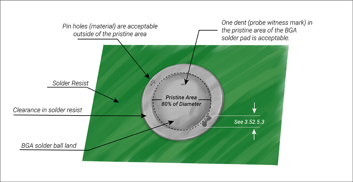
- The external edge defects should not radially stretch towards the middle of the ball land by more than 10% and not more than 20% around the circumference of the ball land.
- One dent is acceptable within the ball’s land.
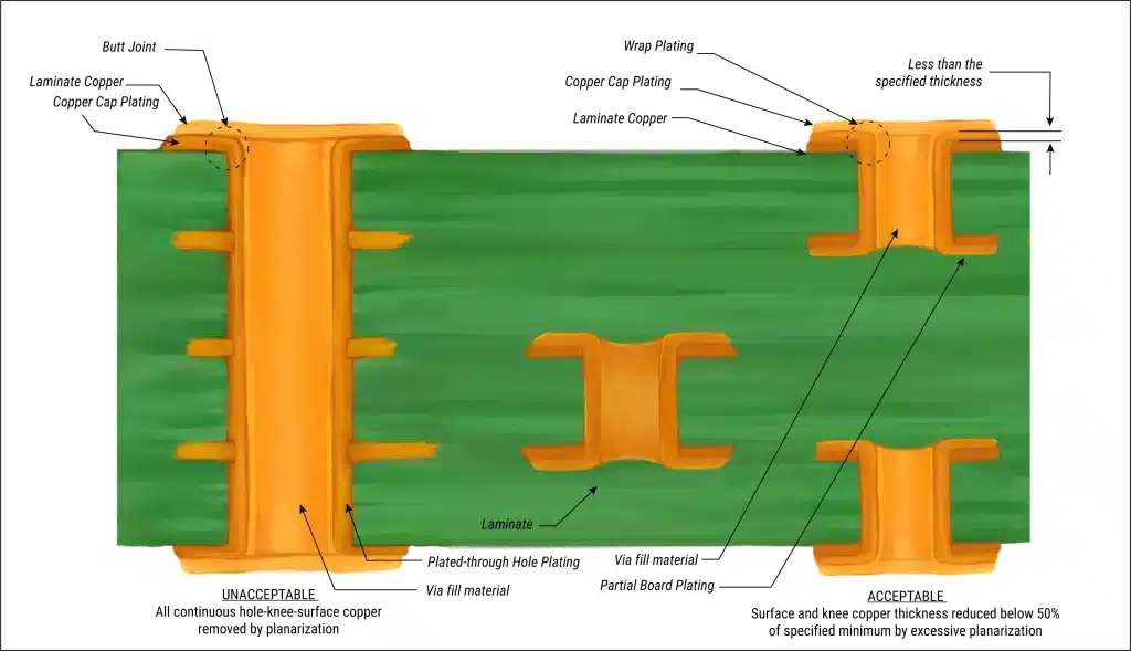
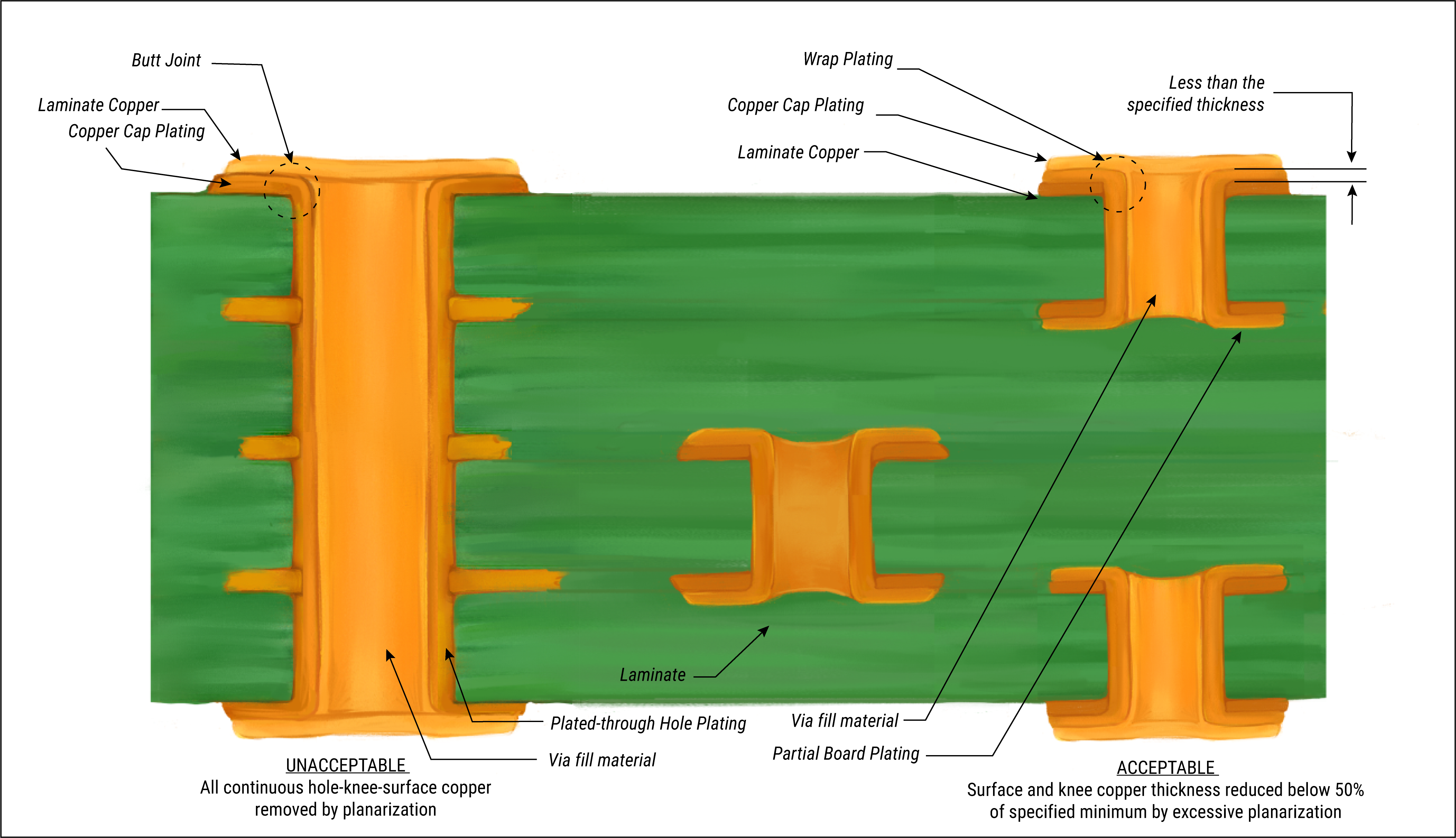
3. Plated through-hole plating
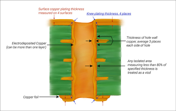
- Copper plating thickness measuring less than 80% of the required thickness is treated as a void.
- Maximum voids per panel shall be 1.
- The plating void should not be more than 5% of the overall PCB thickness.
- There shall be no voids at the interface of the plated hole wall and the internal conductive layer.
The cross-sectional view of a typical plated through-hole post-rework simulation

Acceptable and unacceptable plated-through hole wrap plating for mil-grade PCBs
4. Liquid photo-imageable solder resist considerations
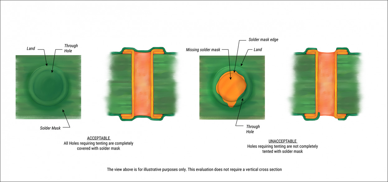
- Holes that require tenting should be completely covered with a solder mask.
- Voids in the solder mask that expose the hole are not acceptable.
5. Via protection in mil-grade PCBs
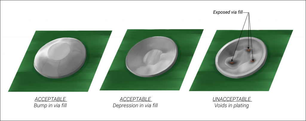
If your PCB design requires copper plating of filled vias:
- There shall be no voids that expose filled vias.
- Bumps and depressions on the copper plating of filled vias are acceptable.
- Voids on the copper plating over the filled vias are acceptable.
Need help in designing reliable PCBs? Our engineering team can help you with thermal management, stack-up design, and DFM analysis.
You can book a meeting with our experts or call us at +1 (800) 763-7503.

Important considerations of a mil-grade PCB design
- Rigid PCB base material: GF: epoxy resin, flame resistant, woven E-glass
- Maximum panel size: 18’’ x 24’’
- Maximum number of layers: 20
- Maximum board thickness: 100 mils
- Minimum hole size: 0.007″ (7 mils) laser-ablated plated hole size before plating, 0.01”(10 mils) drilled the plated-through hole before plating
- Aspect ratio: 0.75:1 for microvias; 10:1 for through-holes
- Minimum conductor width/space: 0.004”/0.004”
- Surface finish: HASL and ENIG
- IPC standard: Class 3 is the highest IPC standard. Mil-grade PCBs should be designed and manufactured based on the standards applicable to class 3 PCBs. These standards include laminate selection, plating thickness, material qualifications, manufacturing processes, and inspection.
Mil-grade parameters for a perfect board
For the best mil-grade board results, stick to the following parameters:
- Minimum dielectric thickness between two planes: 3.5 mil
- Minimum annular ring for inner layers: 6 to 7 mil
- Minimum Annular ring for outer layers: 6 to 7 mil
- Drill to copper clearance: 7 to 8 mil
Note: These parameters are not mandatory, but if followed, your boards will be manufactured close to perfection.
Military-grade PCB design tips
- The components incorporated must match the mil-grade. In contrast to commercial-grade components that have 5 to 10% tolerance, the mil-grade components have a maximum tolerance of 1 to 2%.
- The boards should be capable of handling the maximum current load.
- The low-frequency components should be isolated from the high-frequency ones. This is implemented since the high-frequency components might interfere with the performance of the low-frequency components by inducing noise. Hence, ruining the quality of the signal.
- Shielding of clock signals by creating a material enclosure. These enclosures are generally made of aluminum.
- Quality heat-resistant materials such as Pyralux AP, FR408, and other metallic core components should be used. These materials help withstand high temperatures.
- Thermal compounds should be incorporated for heat dissipation.
- The designer should run pre-layout simulations and impedance checks to understand the behavior of the PCB in real environments.
- High heat-generating components need more clearance than regular components. The increased clearance protects the nearby components and the whole PCB. Hence, the increased clearance should be incorporated at the design stage.
- As annular rings for components and via drills are one of the requirements for mil-spec jobs, ensure that sufficient annular ring is provided in the design.
- The braided wires should be pre-tinned for better solderability.
- The press-fit components must be soldered to prevent vibration.
- Before PCB assembly, the thermal profiles for wave and reflow soldering processes should be verified. This evades component damage during the assembly.
- The right surface finish material should be chosen so that the PCB performs its functionality in rough environmental conditions. The most popular surface finish materials are:
- Electrolytic nickel and gold
- Electroless Nickel with Immersion Gold Coating (ENIG)
- Lead-free HASL
- Immersion silver
- Electrolytic wire bondable gold
- HASL
- To protect the PCB, acrylic-based sprays should be utilized for conformal coating.
- Software simulation programs should be utilized to verify the PCB design. This validates the loads at different locations and helps understand the required design modifications.
- PCB routings should be maintained at 45° angles or less. This assists in smooth current transmission in the circuit.
- While stacking, avoid fragile cores. Designers should carefully pick the type of material that goes into the internal layers. Testing is essential to ensure reliability.
- Impedance consists of two components: reactance and resistance of a circuit. Impedance calculation is critical for testing aerospace and military devices.
- DFT (design for testing) is helpful in the initial layout plan to detect defective boards.
- DFM is a must while designing military-grade circuit boards. It checks the clearances between traces, the aspect ratio of drills, and annular rings as per IPC standards. DFM identifies design violations, helps to resolve all errors, and ensures defect-free manufacturing.
- The aspect ratio affects the reliability of the board. AR (aspect ratio) defines the PCB thickness compared with the via thickness. The recommended maximum AR ratio should typically be between 1:6 to 1:8. Higher aspect ratios threaten circuit board reliability. Moreover, higher AR boards are challenging and expensive.
- Reasonable handling of RF issues- RF interference disrupts the use of specific equipment. Mil-grade PCBs should be designed in such a way that the external RF interference should not affect their performance.
- The metal core boards find substantial use in Milspec/aerospace applications, which generate significant heat and power. Different materials, like aluminum and epoxy-based materials, must be used.
- Make sure the cables are short and have heavy-gauge shields. It is important to check the connectors to verify quality signals and install RFI filters along the signal path.
- Before the assembly, the thermal profiles for the wave and reflow soldering processes are checked. It prevents component damage during the assembly process.
- For high current traces, the width and thickness of the traces should be such that the temperature rise is within the given parameters.
- Military and aerospace PCBs should be manufactured in conformance with MIL-PRF-50884, MIL-PRF-31032, and MIL-PRF-55110 standards.
Populated boards play a major role in maintaining thermal control for Mil-spec/aerospace applications. Focus on the crucial parameters like conformal coating, thermal interfaces, heat dissipation, etc., related to PCBAs for thermal control systems.
- Define the stack-up on the fab drawing for the PCB manufacturing and indicate the required dielectric thicknesses.
The military-grade PCBs undergo uncompromising tests before they are put into use. Before the tests, the designs undergo Design for Manufacturability (DFM). Here, the basic performance and the essential characteristics of the board are tested. The aforementioned design guidance will help the designers to build their prototypes with minimal errors. However, the perfect layout for a military board depends on the application it is designed for.
PCB Transmission Line eBook
5 Chapters - 20 Pages - 25 Minute ReadWhat's Inside:
- What is a PCB transmission line
- Signal speed and propagation delay
- Critical length, controlled impedance and rise/fall time
- Analyzing a PCB transmission line
Download Now
About Rahul Shashikanth : Rahul Shashikanth is an electronics and communication engineer with over 8 years of experience in publishing technical articles on PCB design, manufacturing, and assembly. He is currently the content marketing manager at Sierra Circuits.


