


Contents
Controlled impedance is the characteristic impedance of a transmission line formed by PCB traces and its associated reference planes. It is relevant when high-frequency signals are propagating on the PCB transmission line. In this article, we will demonstrate controlled impedance routing using Altium Designer.
Controlled impedance is important for solving signal integrity issues, which is the propagation of signals in PCB traces without distortion.
Let’s take you through the following steps to achieve the desired impedances for single-ended and differential traces using Altium Designer:
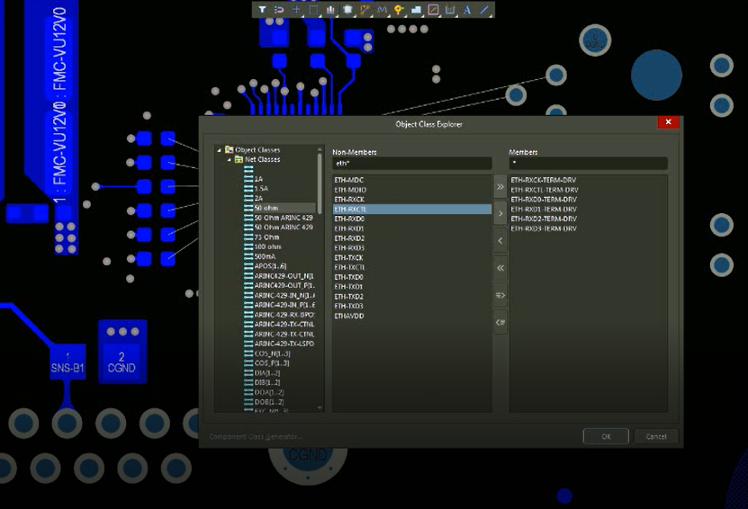
In this demo, we will show you how to route the differential pair with 100 ohms and a single-ended line with 50 ohms. Here, this is the ethernet section with ethernet IC and RJ45 connector.
You can see the net with the receiver (RX) and transmitter (TX) section, RX clock, RX control, and RXD0, D1, D2, and D3. These all are single-ended 50-ohm traces.
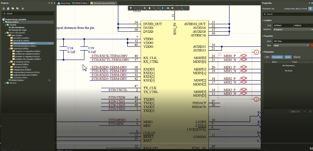
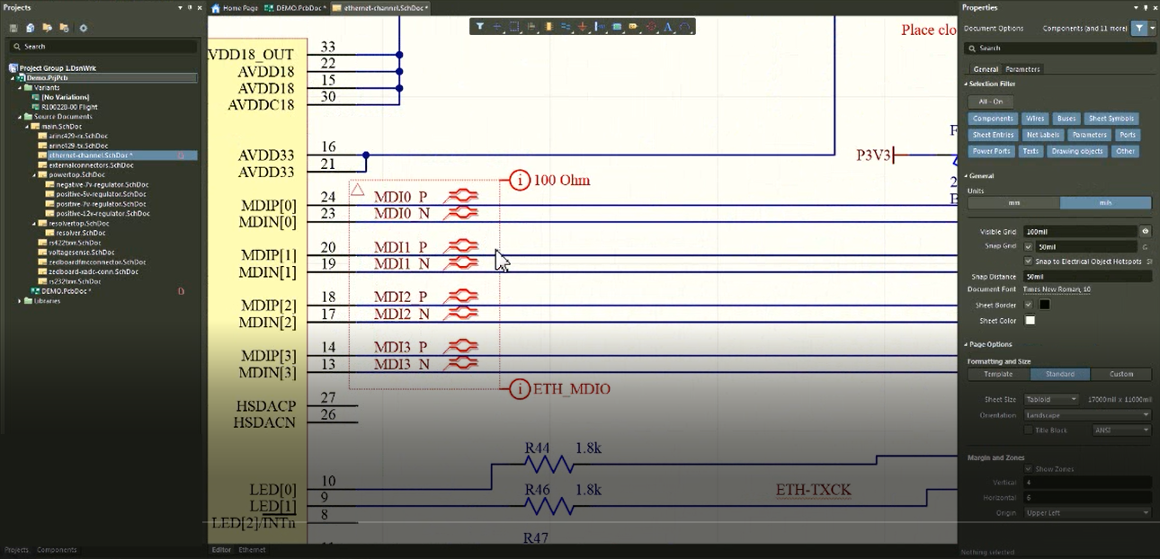
On another side of the IC, you can see an MDI0, one, two, and three. All these connections are 100-ohm differential pairs.
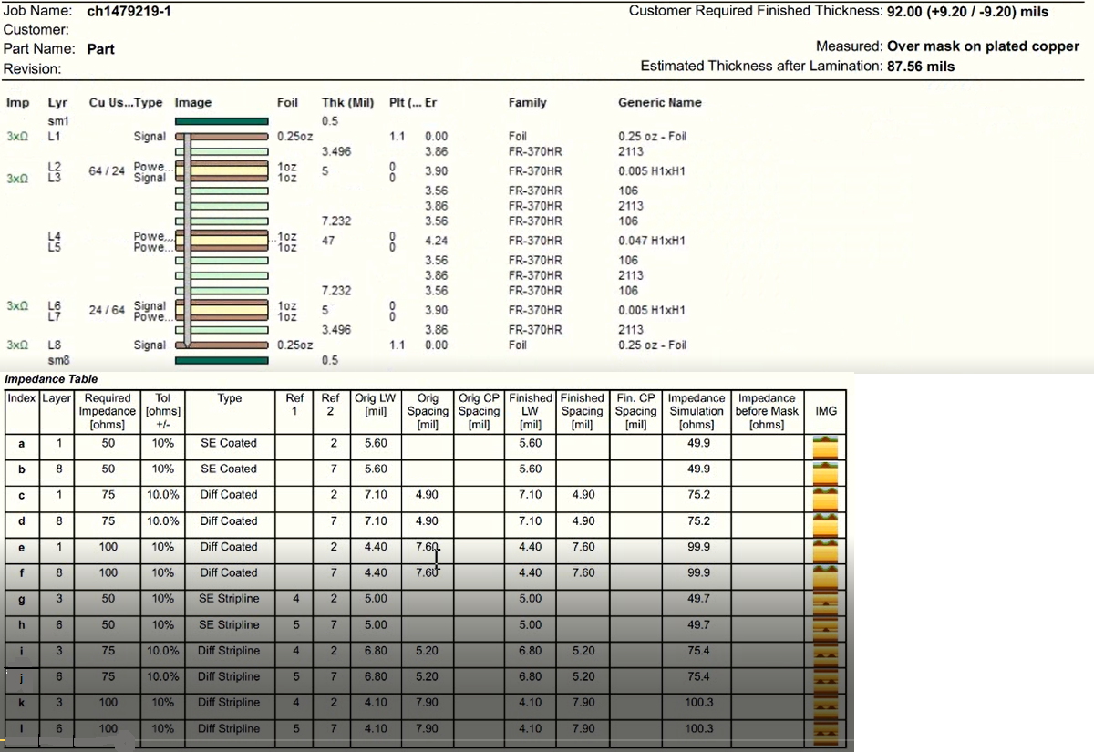
To achieve the impedances, we need certain trace widths; those will be provided by the manufacturer in the form of a stack-up. The image given below is depicting an example of a stack-up. In this stack-up, the layers are given, the required impedances are given, and the trace width and spacing between the traces are also given.

Class creation for controlled impedance routing using Altium Designer
- Go to ‘Design’ >> ‘Classes’ >> ‘Net classes.’
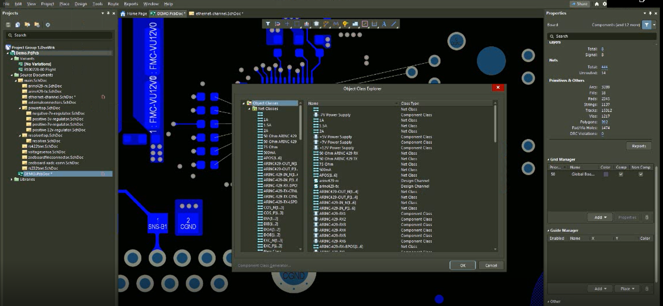
- Right-click on ‘Net classes’ >> click on ‘Add classes.’
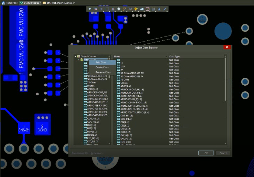
- Give this class a name (100 ohms in our case).
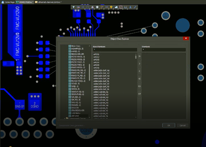
- Go to this 100-ohm class and select the nets which are there in this class and click on the arrow (>).
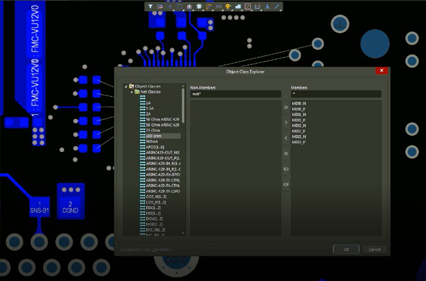
- In this way, all the nets in the class will get assigned to 100-ohm traces.

Controlled Impedance Design Guide
6 Chapters - 56 Pages - 60 Minute ReadWhat's Inside:
- Understanding why controlled impedance is necessary
- Stack-up design guidelines
- How to design for impedance
- Common mistakes to avoid
Download Now
Note: In the same way we will create a 50-ohm class.
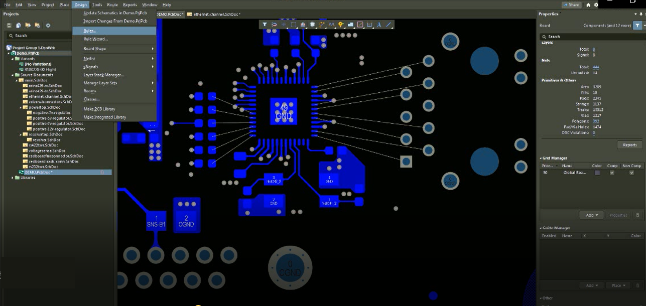
Rule setup for differential pair (100 ohms) routing using Altium Designer
To set the rules for the classes we created above, we will follow these steps:
- Go to ‘Design’ >> ‘Rules.’
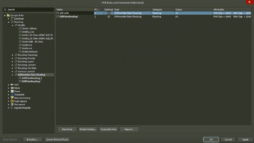
- Go to the ‘Differential pair rules’ >> ‘New rule.’
- Give a name to this rule (100 ohms in this case) and double-click.
- We will now put the values for the top layer, bottom layer, signal one, and signal two. For the top layers in our stack-up, the values are 4.4 mils and 7.6 mils.
- Add minimum width, preferred width, and max-width. The minimum width will be 4.4 mils, and the minimum gap will be 7.6 mils.
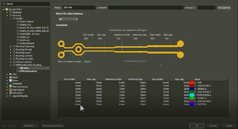

- The impedances are dependent on the trace width and the spacing. Once we do this, we will again go to the stack-up and cross verify the signal one and signal two values. Signal one and signal two values are 4.1 mils and 7.9 mils.
- Add signal one and signal two values. And go to the drop-down box and select a custom query.
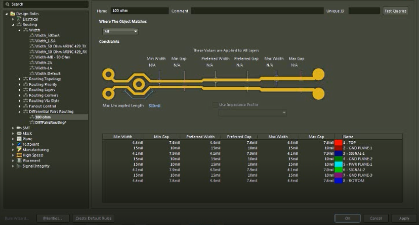
- In the drop-down box, type Net Class and select 100ohms.
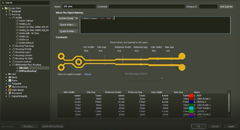
Note: The values in the top layer and the bottom layer will be the same. The ground plane and the power planes are not to be used.
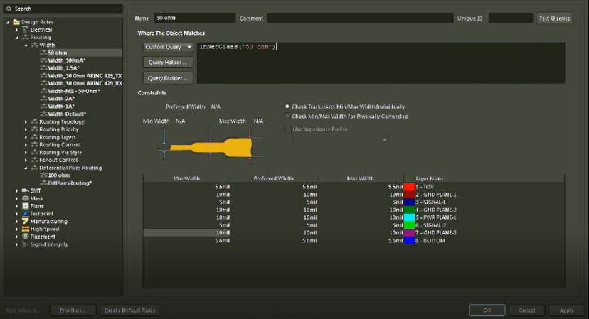
Rule setup for single-ended (50 ohms) line using Altium Designer
- Go to ‘Design’ >> ‘Rules.’
- Go to the ‘single-ended rules’ >> ‘New rule.’
- Give a name to this rule (50ohms in this case) and double-click.
- We will now put the values for the top layer, bottom layer, signal one, and signal two. For the top layer in our stack-up, the value is 5.6 mils.
- Add minimum width, preferred width, and max-width that is 5.6 mils.
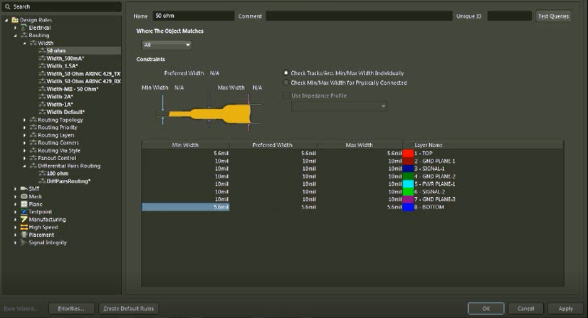
- Go to the stack-up and add the signal one and signal two values that is 5 mils.
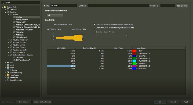
- Go to the drop-down box and select a custom query.
- In the drop-down box, type Net Class and select 50 ohms.

Signal Integrity eBook
6 Chapters - 53 Pages - 60 Minute ReadWhat's Inside:
- Impedance discontinuities
- Crosstalk
- Reflections, ringing, overshoot and undershoot
- Via stubs
Download Now
Differential pair routing using Altium Designer
- For differential pair routing, go to ‘Interactive differential pair routing’ >> ‘Route.’
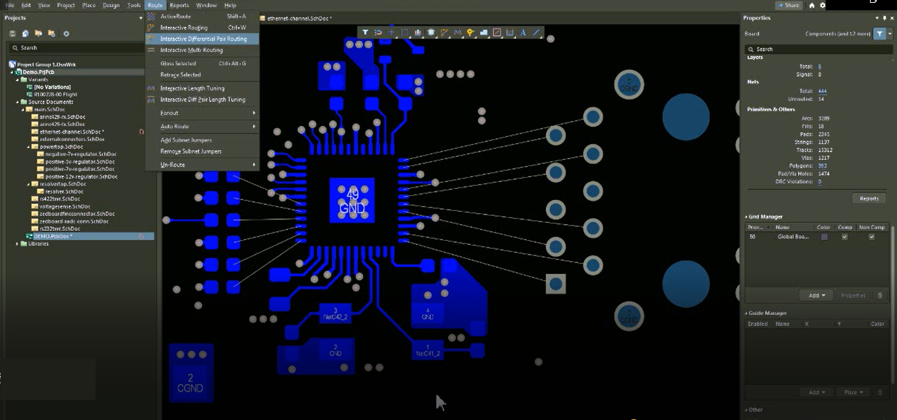
- Now, select the net and do the routing.
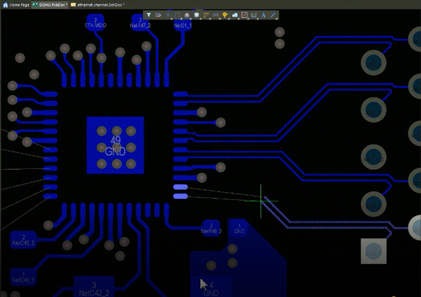
- After completing the routing step, check the values of these particular traces. Select any of the traces, go to properties, and check the values. Here, the trace width is 4.4 mils, which is the same as given in the stack-up.
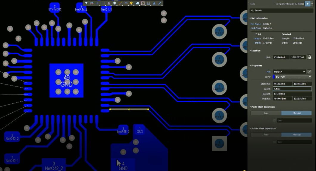
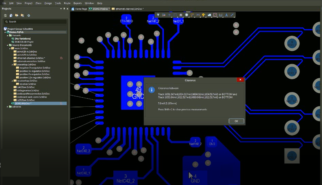
- Now go to report and measure primitives. Select the two traces that will give us the air gap between two traces (7.6 mils), which is the same as the stack-up value.
Single-ended routing using Altium Designer
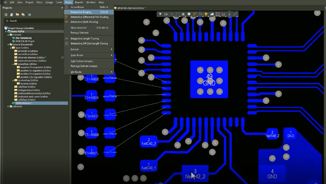
- For single-ended routing, go to ‘Interactive routing’ >> ‘Route’ and repeat the above steps.
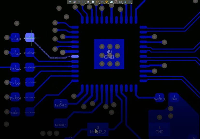
- Once the routing is done check the trace width.
- Select the trace under properties. You will see the trace width is 5.6mils that is the same as given in the stack-up.
Layers contain controlled impedance that is why we need to specify these impedances in the fab notes since there can be more than one value of impedance traces per layer. Separate aperture codes are defined for controlled impedance traces. Trace impedance is a critical factor in the effort to transmit signals without distortion over a trace. Impedance must match the drivers and the load. We hope that our tutorial on controlled impedance routing using Altium Designer helps the designer to understand and follow the minute details while routing their PCB.


