


Contents

On-demand webinar
How Good is My Shield? An Introduction to Transfer Impedance and Shielding Effectiveness
by Karen Burnham
Cost control steps should be taken in the early PCB production stages, including the actual circuit development stage. Be aware of the process steps and cost drivers for rigid circuit boards because each process consumes additional cost in terms of process time, materials used, energy, and waste treatment.
We need to keep in mind the production strategy, production equipment, and multiple technologies to control the rigid circuit board cost. In this blog post, we would like to indicate the essential PCB features, including process and manufacturing steps involved in the PCB production based upon their impact on cost.
Key cost drivers for rigid circuit boards
Process cost affects the final PCB price, and once the PCB is designed, you cannot reduce it without redesigning the board. The lowest possible cost of circuit board can only be achieved by adopting accurate PCB design and the right engineering tactics. Follow IPC-2220, IPC-2226 standards if you want to optimize the cost.
PCB processing cost considerations

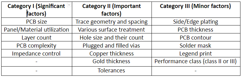
We have divided the cost contributing elements into different categories. The motive of this classification is to reduce the final cost. We cannot neglect the factors listed in category I but we can change the factors listed in II and III based on our requirements and end application.
For PCB designers and engineers, optimization is the prime factor. Optimization of time, cost, and even effort. Sierra Circuits strives to provide customers with high-quality PCBs and excellent design service. This includes best practice tips for designers. When designing your next circuit board, you need to watch some crucial rigid PCB cost drivers.
From the concept to the PCB fab and assembly, several factors impact the price of your board. Typically, the mechanical and/or electrical engineers determine the board requirements such as the size, the applicable industry standards, the mechanical and electrical constraints, and material properties. And it is done to ensure that the board meets its targeted performance.
Once the engineers have a mechanical design that works and a functional schematic, the PCB designer must do the CAD layout. When the layout is completed, the PCB manufacturer can start building the board. It goes without saying that the complexity of a design will have the most significant impact on the final cost of a circuit board, but the price will also mostly depend on the following cost drivers. Read our post on computer-aided manufacturing (CAM).

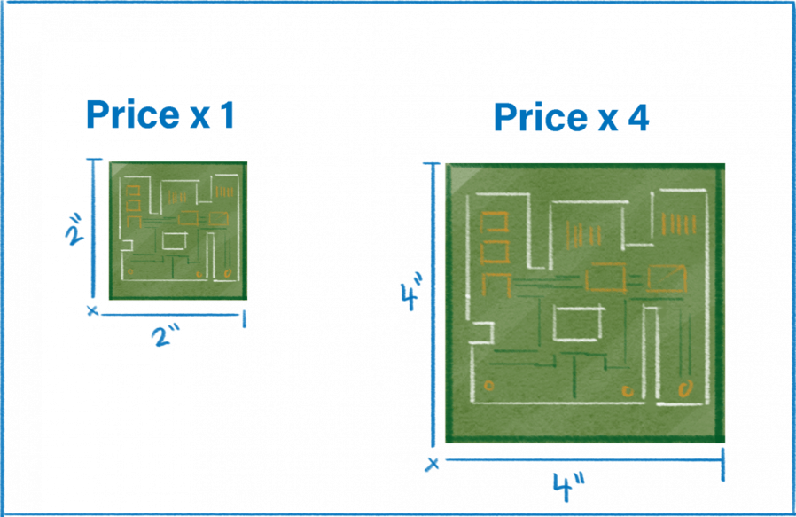
The size of the PCB
The mechanical engineer has to determine the size and the shape of the PCB – also called the PCB outlines. The initial drawing is sent to the design team, who can reduce the board outlines if possible. This is the first way to save money since a smaller area reduces the PCB material cost. Here, the cost of your board is a real estate issue – just like a home, the bigger it is, the more it costs. For example, imagine a 2’’ x 2‘’ board. Now imagine a 4’’ x 4’’ board. The surface area has been multiplied by four, therefore the base price (for the material) will also be multiplied by four.

The bigger the panel, the more it costs
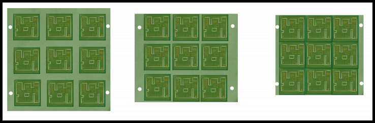
When you pick a panel option, keep in mind that it is just like the board size. The bigger the surface area is, the more it will cost you. So, you even pay for the waste part (in faded green) that is thrown into the bin after assembly. If possible, place the boards on the panel closer to each other to reduce waste and cost.
To sum up, the hard cost drivers you should take into account during the concept stage are the PCB outlines, the layers, and their traces/space and vias. Carefully select the types of material you need and try to avoid waste as much as possible. Finally, keep in mind that reducing machine time (for both manufacturing and assembly) will also reduce the cost.
Array considerations: It is a good practice while using a panel for maximum yield. Let us understand it with some examples:
Example 1: Size of the panel = 18 x 24”
Array size = 5.125 x 10.925”
Size of the array part (four parts in each array) = 2 x 4.9”
Panel yield: There are a total of 6 arrays, i.e., a total of 24 parts. Material utilization is 77.8%. It signifies good utilization of the material on the given panel.

Example 2:
Size of the panel = 18 x 24”
Array size = 11.125 x 5.125”
Size of the array part (four parts in each array) = 5 x 2”
Panel yield: There are a total of 4 arrays, i.e., a total of 16 parts. Material utilization is 52.8%. It signifies poor utilization of the material on the given panel. It increases the cost by 33% in comparison to 24 parts per panel in the previous example.


Design for Manufacturing Handbook
11 Chapters - 96 Pages - 90 Minute ReadWhat's Inside:
- Annular rings: avoid drill breakouts
- Vias: optimize your design
- Trace width and space: follow the best practices
- Solder mask and silkscreen: get the must-knows
Download Now
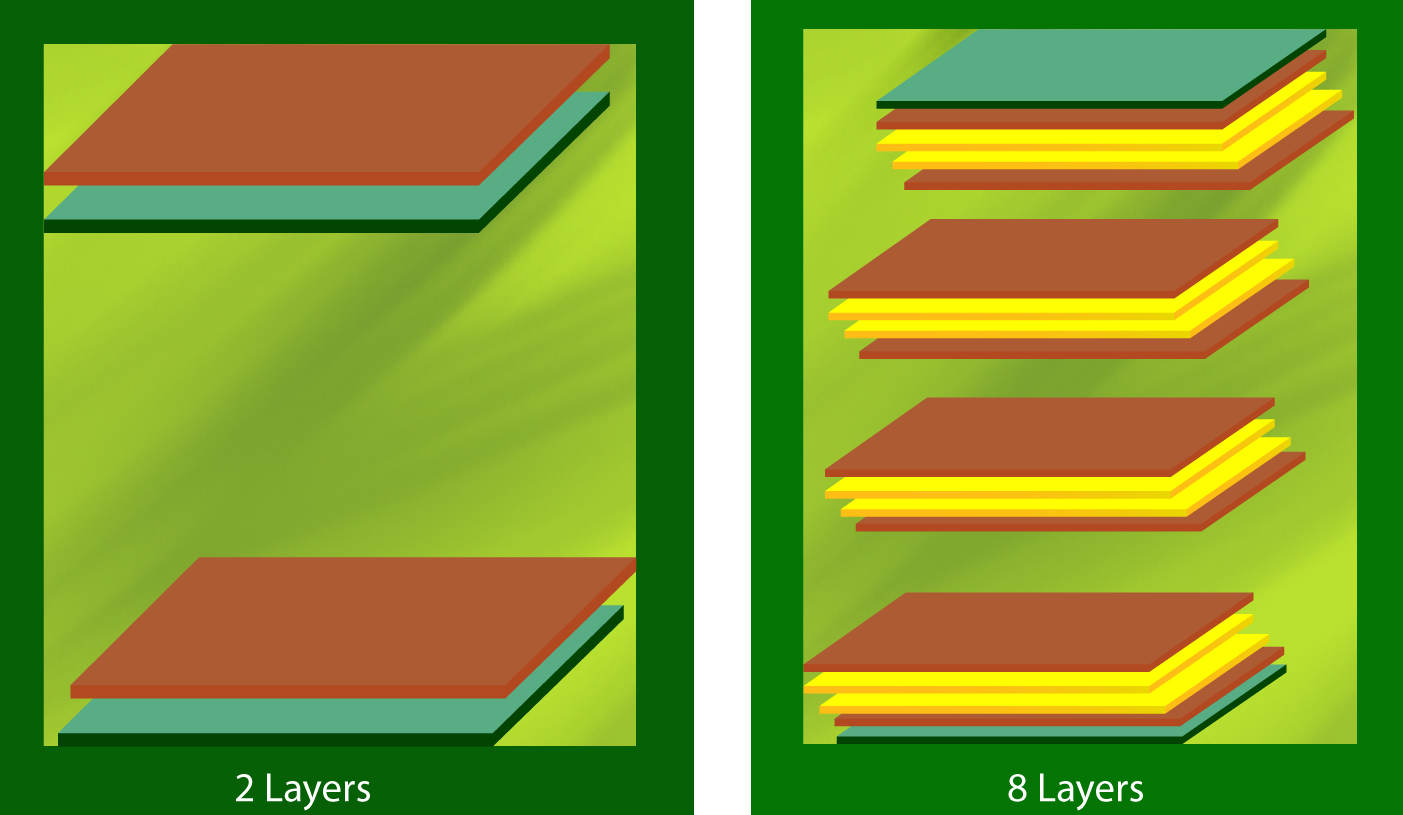
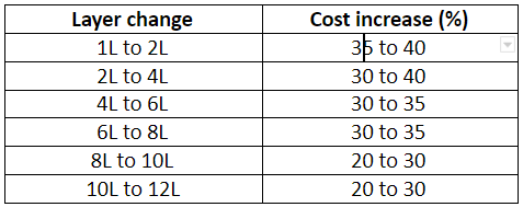
More layers mean more production time, more production steps, and more material
Naturally, more layers mean higher costs. Additional two layers will increase costs by about 25%. As you add more layers to your design, you add more material, like prepreg and copper, and more production steps, like etching, pressing, and bonding cycles, etc. And once produced, the layers have to be inspected. It is more work to inspect eight layers than it would be only to inspect two.
Layer count can be reduced by using HDI (high density interconnect) technology. But be careful; if you are not an experienced designer in HDI, it is recommended to first understand the key aspects of HDI. You can read our article on HDI cost advantages.
Cost goes up with the complexity of the PCB
The cost increases when we shift from a conventional PCB manufacturing technology towards a complex one. This inclination for more complex technology comes due to the end application requirements. But a manufacturer should decide wisely so that cost could be minimized. Always choose turnkey PCB manufacturing and assembly from a single facility for a cost-effective and quickturn solution of your designs.
- Interconnect size scaling: As soon as the size of interconnects reduces to meet the application requirements, the cost increases.
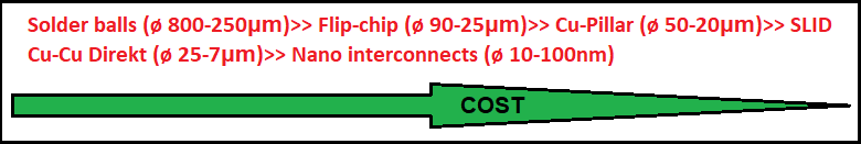
- Microvias: Implementation of microvia structures broadly impact PCB manufacturing because they directly affect the total number of lamination cycles and drilling steps in a design. It happens during sub-constructions where microvia start and stop layers need to be considered. And it eventually increases the cost since each sub-construction requires extra laminations and drilling cycles.
The copper foil weight
In general, the thinner the copper is, the less expensive the circuit board is. Using thick copper on your inner layers will require more prepreg during lamination to fill up the gaps between the areas made up of copper. More than ½oz of copper on the inner layers and more than 1oz of copper on the outer layer increases the PCB cost.
Another disadvantage of using thicker copper is that you have to maintain significant spaces between traces, and you could also need thicker prepreg materials between two adjacent layers. However, if you use very thin copper (less than ¼oz), it adds extra cost since processing very thin copper is expensive.
The trace/space
The tighter your trace/space, the more difficult it will be to etch your traces and pads reliably. Take into consideration whether a wire bonding or HDI design will be more cost-effective in the long run. Sierra Circuits can manufacture sub 3/3 trace/space.
The more number of drill holes and smaller the holes the more it costs
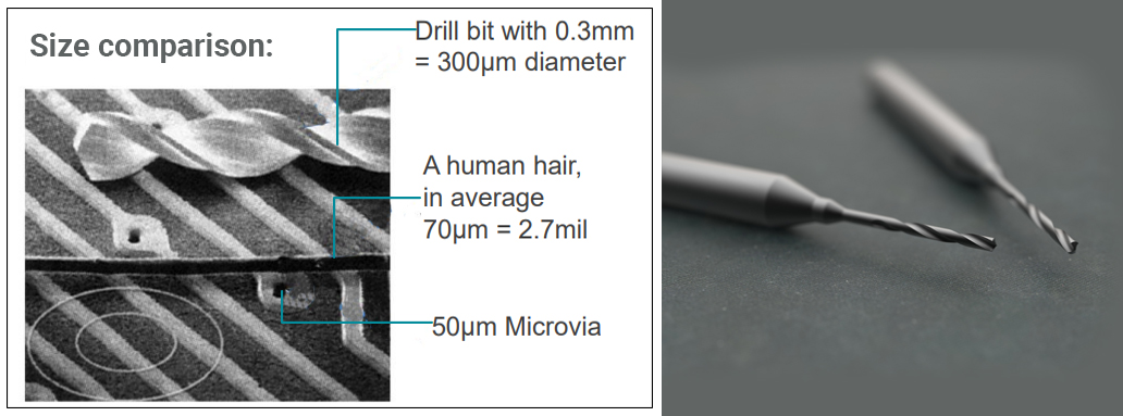
Smaller mechanical hole sizes are more difficult to manufacture. They also require smaller drill bits, which cost more. And when you request a hole smaller than 6mils, it usually has to be laser drilled, which drives up the cost.
HDI PCB technology uses blind and buried vias, which add considerably to the cost of a circuit board. They are more difficult to drill than through-holes and also add lamination steps. Only use them when you don’t have any other options available. For example, it makes sense to have these kinds of vias in an HDI design due to the PCB size constraint. If you are facing trouble routing traces, then adding another two layers to the stack-up will be cheaper than using blind or buried vias.
The standard drill bit size is 8mils, whereas the advanced drill bit size is 5mils. And the R&D drill bit size could be less than 5mils. Note that small hole size and thick PCB (high aspect ratio) increase drilling time and the drill erosion, resulting in a higher cost.

HDI PCB Design Guide
5 Chapters - 52 Pages - 60 Minute ReadWhat's Inside:
- Planning your stack-up and microvia structure
- Choosing the right materials
- Signal integrity and controlled impedance in HDI
- Manufacturing considerations for higher yields
Download Now
The drill to copper
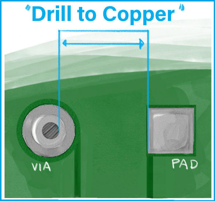
Drill to copper is the distance from the edge of the drilled hole to the nearest copper feature on a layer (pad, pour, and trace, etc.). The smaller the drill to copper, the more expensive the PCB manufacturing process is.
Controlled impedance
Having a controlled impedance means designing and producing very specific and uniform trace widths and space. More expensive materials with specific dielectric properties have to be picked to ensure that the targeted electrical performance is achieved. Test coupons have to be fabricated to ensure that the PCB manufacturer met the standard 15% tolerance. Sometimes, it is even 5% tolerance. More work, more surface area for the coupons, and more testing drive up the price of the board.
Do not specify controlled impedance unless it is absolutely necessary. That is the reason we have put this in the significant category.

Material selection criteria for rigid circuit boards’ cost optimization
- Lead-free solder compatible (thermal reliability)
- TG (temperature-related reliability)
- TCT, CTEz (temperature cycle reliability)
- Degradation temperature (thermal reliability)
- High thermal conductivity (heat transfer)
- T260, T288 (time to delamination)
- εr (Dk), Df (electrical signal performance)
- CAF resistant
- Mechanical properties (Drop test, stiffness, etc.)
- Halogen reduced (environmental features)
Choice of material
When we move higher in the frequency chart to be application-specific, the choice of PCB materials becomes crucial.
Cost control must be considered in the early phase of PCB design. Smart design and sound engineering are always the best PCB design solutions with the lowest possible cost index. For the most accurate cost estimate, it is advisable to consider an existing design scope and then adjust the requirements based on the estimated technologies. These estimates will provide more relative data points to make any cost per technology decision and prevent surprises later in the process when resources have been committed to a design.
We are all involved in the supply chain for every unique PCB, and we have the expertise that can bring your products to market as quickly and as well-engineered as possible. But please note this has to be considered as early as possible within the supply chain.
Additionally, ordering PCB prototype and bulk production from a single fab house can help you reduce supply chain risks and the overall cost.

PCB Material Design Guide
9 Chapters - 30 Pages - 40 Minute ReadWhat's Inside:
- Basic properties of the dielectric material to be considered
- Signal loss in PCB substrates
- Copper foil selection
- Key considerations for choosing PCB materials
Download Now


