


Contents
You can place an order for circuit boards using various online and offline platforms depending upon the manufacturer’s services. Knowing about what happens once you place your PCB order is vital as it helps you to understand the status of your order.
See the benefits of ordering PCB fab and assembly:
To learn more about the advantages of turnkey PCBs, see the benefits of choosing turnkey PCB manufacturing and assembly from a single facility.
Once your order is placed, we will analyze the fabrication and assembly data you’ve provided as the initial step in circuit board manufacturing. We not only ensure we have all the required information but also check for design flaws that could cause manufacturing delays. We guarantee a quick turnaround thanks to our streamlined manufacturing and delivery, and our ability to serve as a single point of contact throughout.
For NoTouch PCB orders, quotes are received and either approved or denied by our AFV tool. Denied quotes receive instructions via email (rejection reasons) on why the quote was denied, and how to fix the errors. For all other orders, once the quote enters our system, expert design engineers will examine and verify the manufacturability and reliability of the board. If the order is partially turnkey or consigned, further instructions will be emailed.
In this article, we have outlined the procedure that we follow once your PCB order is submitted.
PCB manufacturing
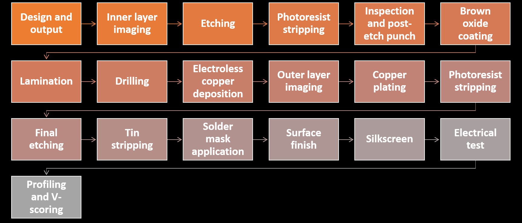
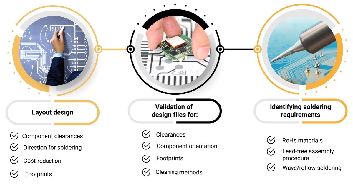
Circuit board manufacturing is the process of converting design files such as Gerbers and netlists into a physical circuit board on which components are assembled. The manufacturing process begins with design files such as Gerbers/ODB++, netlist, drill files, etc. We perform DFM checks to identify potential errors that may occur during the fabrication process. In case of any errors, you will be informed about them and guided to make the necessary corrections.
The error-free design files are sent to the CAM team, who will create various output files such as drill files, imaging layers, solder mask files, etc.
If your board has more than two layers, inner layer imaging on a PCB core will be done first. During this process, a special printer called a plotter is used to create the images of the circuit, solder mask, and silkscreen layers. This panel also consists of a layer of photoresist that polymerizes when exposed to UV light. The computer scans the surface of the board and turns it into a digital image. After developing the image, an alkaline solution is used to remove the unhardened photoresist (which protects the desired copper). After removing the photo-resist, the board will be scanned by an automated optical inspection system (AOI) to verify the circuit image.
Once the image is verified, the copper circuit will be coated with brown oxide to prevent corrosion. This process is repeated to all the inner layers and will be laminated together with the outermost layers. After the lamination process, the board will be sent to hole creation (drilling), copper deposition/plating, solder mask application, surface finish, and silkscreen application.
For a detailed explanation, see our post, How is a PCB manufactured?
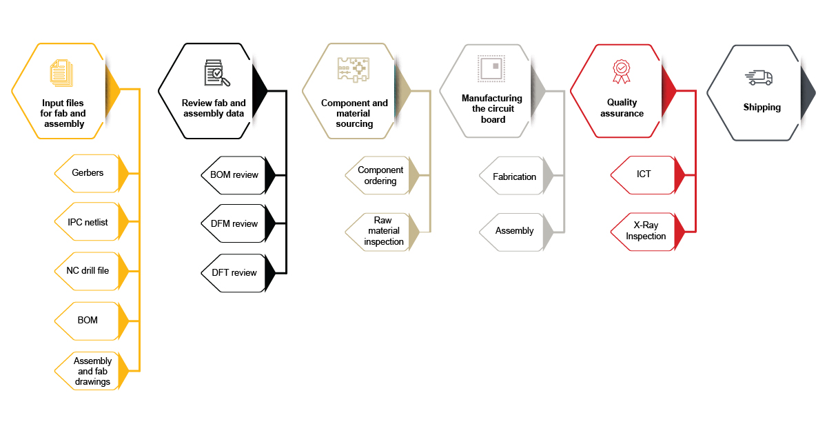
Input files for fabrication
Board manufacturers require certain design files to carry out the fabrication process. A few important ones are listed below:
Gerbers / ODB++
Gerber/ODB++ files are digital blueprints of a PCB that contain layer-by-layer details required for manufacturing. These files come in open ASCII vector format and describe the physical attributes of each board layer.
IPC netlist
It has a list of networks that forms the conductivity interconnection scheme of the board. It is an ASCII text file with the CAM system instructions including the net names, pins, and X-Y coordinates of the start and endpoint for each net/node.
NC (numerically controlled) drill file
These files are used to define board drilling and routing data. The drill file refers to the position, size, and the number of holes in a board.
Fabrication drawing
Fabrication or fab notes include board dimensions, drill details, class of fabrication (class 2, class 3), stack-up details, etc. These drawings are sent in a PDF format to the manufacturer. This also includes any specifications related to dielectric materials to be used.
PCB assembly
We will first review your design data before beginning the assembly process and ensure that the design is manufacturable. This will include DFA parameters such as component placement clearances and suitable thermal reliefs. In case of any discrepancies, our engineers will collaborate with you and make the board manufacturable.
Once the data is verified, we secure the fabricated bare boards and bake them to remove moisture. Later, the components are fetched either from our inventory or from an external provider.
The next phase of circuit board assembly is applying solder paste to the boards that have surface mount components. This is generally done by creating stencils from the CAD data. To expedite this process, we use a solder jet which is a programmable device. This machine ensures precise application of the solder onto the board, improving the accuracy and eliminating the cost of stencils.
This is followed by placing components on the board. Through-hole components can be mounted manually or with the help of software-controlled machines. In the case of high-density pin components, manual insertion is the only option due to the components’ unique shape and size. Solder paste holds these components in place.
Once the components are placed, they will undergo various soldering processes such as wave soldering and reflow soldering. The soldering technology depends on the type of components you choose to place on your board.
BOM (Bill of Materials)
The bill of materials contains the list of components and their specifications required for assembly. This file includes the manufacturing part number (MPN), vendor part number (VPN), part quantity, value, do not install (DNI) parts, reference designator, footprint, etc.
We will double-check that to ensure it matches the design’s parts. It’s possible that the BOM is out of date if it hasn’t been updated with the most recent design information.
The next stage is to make sure that the components are available for manufacture at a reasonable cost. If this is not the case, the engineering team will suggest part substitutions or even design adjustments to incorporate preferred components.
Also see the PCB procurement checklist for hardware engineers to avoid stockouts, obsolete components, and last-minute part substitutions.
Component and material sourcing
Once we verify the design data, component and material procurement begins. If you have requested a quote for an order with consigned assembly, you will have to supply components in accordance with our kitting guidelines. We will acquire everything needed for turnkey orders through our specialized buyers and component engineers, eliminating miscommunications that often occur when working with multiple vendors.

How can I tweak the design after placing the order?
There can be an instance where you may need to make changes to your design post placing your order. You can certainly raise this request by contacting your account manager. Your order will be placed on hold as per your request. After this, you will have to share the new set of data with us. The difference between the old and new data will be analyzed. The changes will be incorporated if the job is in the stage where we could implement the proposed change.
For instance, if the customer has requested a change in an outer layer pad dimension, and we are still processing the inner layer imaging, the engineering team will update the data as per the customer’s request in our system and will incorporate these changes once we arrive at outer layer job.
Parameters that are checked during board fabrication and assembly
Design for manufacturing (DFM)
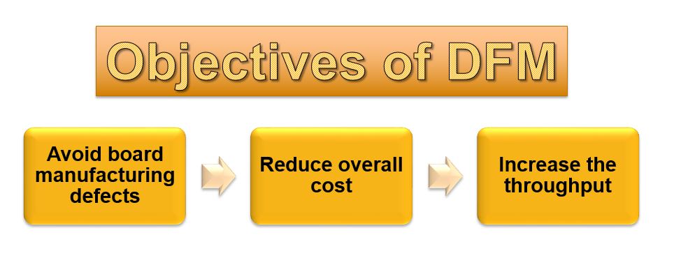
One of the primary objectives of DFM is to avoid manufacturing snags during the board design stage. Faster turnaround times, higher quality boards, and reduced costs are all among the advantages of DFM. In this stage, we watch out for incomplete design files, trace-width and spacing violations, open traces, drill to copper, and solder mask infringement.
To get an advanced overview of the design aspects that impact the manufacturability of your board, see our Design for Manufacturing Handbook

Design for Manufacturing Handbook
11 Chapters - 96 Pages - 90 Minute ReadWhat's Inside:
- Annular rings: avoid drill breakouts
- Vias: optimize your design
- Trace width and space: follow the best practices
- Solder mask and silkscreen: get the must-knows
Download Now
Design for assembly (DFA)
During this stage, we validate each component’s source carefully to ensure its authenticity. Unauthorized sources increase the risk of delays, misinformation, and counterfeit parts.
We check the following design aspects during DFA:
- Size, spacing, and tolerances for drilled holes are within the capability
- Board edge clearance rules are followed
- Board shape allows for optimal panelization
- Thermal reliefs are incorporated wherever necessary
Design for testing (DFT)
The testability of the design will also be examined. This is an important step at the end of the production process to ensure that the assembly was performed accurately. It includes potential test points on the board, the presence of test fixtures, and software as needed. Our engineering team will check the PCB layout for potential areas of improvement in order to improve testability and coverage. We also develop or modify test setups as needed.
Raw material inspection
After receiving the components, and materials, they will be inspected for quality and acceptance.
During the inspection, the components will be checked for cracked cases, apparent damage, bent or broken leads, and other issues such as improper markings or out-of-date parts. The pieces are enlarged using optical equipment, and the results are meticulously documented for tracking. Although it is impossible to inspect every component that will be utilized, we will sample test new components as they arrive until the component vendor has been verified as a reliable source.
Quality assurance
Quality testing is up next. We vet the manufactured circuit boards in accordance with IPC-A-610, IPC-A-612, and IPC-A-613 assembly standards. Our operations also meet the requirements for certifications including ISO:9001:2008, ISO:13485:2003, and the restriction of hazardous substances directive (RoHS). We are also ITAR-registered.
X-ray inspection
Finally, the completed board undergoes X-ray inspection. For example, after assembly on the single- or double-sided ball grid array or micro-BGA installation, the boards are X-rayed 100 percent to ensure integrity.
Shipping
Once the board passes all the tests, your order will be shipped to your address through our courier partners.
Sierra Circuits’ manufacturing and assembly standards are aligned for prototyping and production of circuit boards for industries such as aerospace, medical, and automotive. If you have your design files ready, upload them on our custom quote web app and get your quote instantly. Please let us know in the comments section if you require more information on how to order a PCB.

PCB Design for Assembly Handbook
6 Chapters - 50 Pages - 70 Minute ReadWhat's Inside:
- Recommended layout for components
- Common PCB assembly defects
- Factors that impact the cost of the PCB assembly, including:
- Component packages
- Board assembly volumes
Download Now
About Amit Bahl : Amit Bahl, widely recognized as the PCB Guy, earned his Bachelor of Science in Engineering from UCLA. He is currently the Chief Revenue Officer at Sierra Circuits, where he continues to lead efforts to simplify the PCB design journey and support designers and engineers in creating high-quality boards.


