


Contents
The digital world is getting complex hour by hour whereas the hardware associated with it is getting drastically smaller. The advantages of HDI PCBs are numerous, starting with more interconnections in smaller areas. This results in the miniaturization of boards that can be used in many applications.
Your computers are no longer heavy. They are sleek and sexy. You can work on your laptop and keep your business running while you board a flight. You can also watch your favorite action movie on your smartphone, some of which are way powerful than your laptops. Or you can just plug in your wireless headphones and get into the groove. Mankind is fond of electronics and it has become a part of our lives. In this era, all the electronic devices are designed for portability. Electronic devices are being designed for human convenience. All this was possible because of the miniaturization of the components and PCBs inside the electronic devices.
The PCB industry plays a prominent role in the development of all the electronic gadgets. Let it be a pacemaker in someone’s chest or the motherboard in a programmer’s workstation, PCB made it possible for creating crucial electronic devices.
As the size of the components shrinks, printed circuit board manufacturers adapted to the changing trends. This led to the birth of HDI design. This has PCBs smaller, denser with higher component count, and faster.
We will cover the following topics in this blog post:
- What is HDI PCB?
- What Are the Advantages of HDI PCBs?
- HDI PCB design tip
- The difference between HDI and standard PCBs
- Understanding HDI stack-up and via Construction
- Lamination process and the different types of HDI PCB stack-ups
- What are the applications of HDI PCBs?
- Designing using HDI
What is HDI PCB?
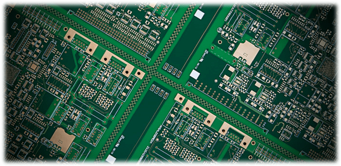
High-Density Interconnect (HDI) is simply a PCB with more number of interconnections, occupying minimal space. This results in the miniaturization of the circuit board. The components are placed closer and the board space is significantly reduced but the functionality isn’t compromised.
To be more precise, a PCB with an average of 120 to 160 pins per square inch is considered as an HDI PCB. The HDI design incorporates dense component placement and versatile routing. The HDI popularized microvia technology. A denser circuitry is crafted with the implementation of microvias, buried vias, and blind vias. The drill to copper is reduced in an HDI design.

HDI PCB Design Guide
5 Chapters - 52 Pages - 60 Minute ReadWhat's Inside:
- Planning your stack-up and microvia structure
- Choosing the right materials
- Signal integrity and controlled impedance in HDI
- Manufacturing considerations for higher yields
Download Now
What are the advantages of HDI PCBs?
-
- Phenomenal versatility: HDI boards are ideal where weight, space, reliability, and performance are primary concerns.
- Compact design: The combination of blind vias, buried vias, and microvias brings down the board space requirement.
- Better signal integrity: HDI incorporates via-in-pad and blind via technology. This helps in placing the components closer to each other which cuts down the signal path length. The HDI technology removes via stubs and therefore reduces reflections of signal and thus improving signal quality. It therefore remarkably improves signal integrity due to shorter signal paths. Also read: Signal Integrity: Via Stubs and Their Effects on Signal Attenuation and Data Transfer Rates
- High reliability: The implementation of stacked vias make these boards a super shield against extreme environmental conditions.
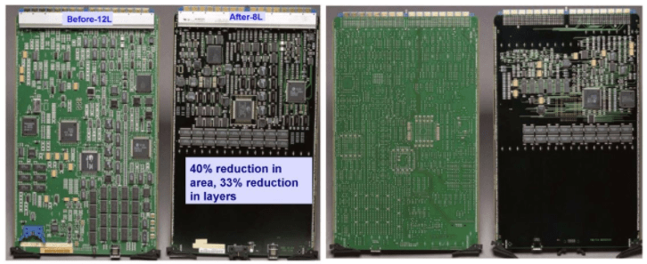
- Cost-effective: The functionality of a standard 8-layer through-hole board (standard PCB) can be reduced to a 6-layer HDI board without compromising the quality.
To understand the hidden economy of HDI, see how HDI boards can be more economical.
HDI PCB design tip
Once you determine that you require HDI, you need to look at the stack-up. Don’t use more than three sequential layers unless there is absolutely no other solution. It is recommended that you use a good fanout strategy for complex ICs, like BGAs and QFNs – this will help you reduce the number of sequential laminations if you plan your fanout strategy properly. Read how to avoid crosstalk in HDI substrate.
The difference between HDI and standard PCBs
HDI inherently provides a better signal integrity performance than non-HDI because all the stray capacitances and inductances get reduced when using small blind and buried vias. Since there are no stubs, the impedance of microvias is close to the trace impedance. The stray capacitance of a normal via is much higher, which causes a greater discontinuity in impedance than a microvia does. Some of the significant differences between the HDI and conventional PCBs are listed below:
HDI PCB |
Standard (Through-hole) PCB |
|---|---|
| Higher component density per square inch | Lesser compared to HDI |
| Smaller, lighter boards with more functionality | Larger and heavier boards |
| Implementation of Blind, buried, and microvias | Through-holes |
| Laser direct drilling | Mechanical drilling |
| Lower number of layers | Higher number of layers |
| Compatible with high pin count and low pitch packages | May face compatibility issues with low pitch packages |
Understanding HDI stack-up and via construction
Happy Holden, the author of the HDI Handbook, explained:
”It took us 10 years designing HDI boards at HP before we realized that these “were more than small through-holes.” We kept designing TH multilayers and using the small-laser-drilled blind vias in BGA breakouts in place of the larger drill TH vias. Then we realized that at a rate of >600 vias/second, 20,000 laser-drilled holes (or 200,000) costs the same as 200 laser-drilled holes. We then started to figure out ways to replace any mechanically drilled hole with a laser-drilled one.
We also discovered that there was room to put 2 laser-drilled blind vias between the lands of a BGA where we had space for only one TH before. This led us to discover ‘channels’ and ‘boulevards’ created by the placement of these blind vias on the inner layers. Channels and Boulevards are the ‘secret’ to obtaining 2X to 4X routing density on inner layers, which means you can reduce the number of signal layers which also leads to the reduction of the number of reference planes.
Go back and look at past HDI boards you have built and measure their ‘pins/sq in’ and ‘in / sq inch’ wiring on each layer, as well as future builds and create a ‘table of your own’ to give to people.”
To learn how to address routing issues in high-density circuit boards, see 5 HDI PCB routing challenges with solutions
Lamination process and the different types of HDI PCB stack-ups
HDI PCBs are multilayer boards that are constructed with densely routed layers. The boards are held together through lamination process and the layers are electrically interconnected using different types of vias.
The process of lamination begins with the etching of the inner copper layers. Later they are separated by partially cured laminates and stacked like a book with layers of prepreg on the top and bottom. The stack-up is then pressed and heated enough to liquify the prepreg. These liquified prepregs cool down and stick the layers together.
For blind and buried vias stack-ups the PCB will undergo several numbers of sequential laminations. The more the number of laminations, the costlier will be the board.
To increase routing density, designers increase the number of layers, producing a complex stack-up. Manufacturers use sequential lamination processes to fabricate such complex designs.
Some of the common types of stack-ups are mentioned below:
- 1+N+1 – PCBs contain 1 build-up of high-density interconnection layers
- i+N+i (i≥2) – PCBs contain 2 or more build-up of high-density interconnection layers. Microvias on different layers can be staggered or stacked
- i+bN+i (i≥2) – Includes buried vias
- Any layer HDI – All the layers of a PCB are high-density interconnection layers. This allows the conductors on any layer of the PCB to be interconnected freely with copper filled stacked microvia structures
What are the applications of HDI PCBs?
Healthcare
The HDI PCB is making an impact on the medical industry. The medical devices are usually HDI since they can fit in small devices like implants and lab and imaging equipment. Medical equipment plays a crucial role in diagnosing diseases and also do provide life support. Ex: Pacemaker, Diagnostic and monitoring facilities.
With the miniaturized camera sizes, the inner parts of the patients can be observed and the right diagnosis can be established. The cameras are getting smaller but the picture quality isn’t compromised. The HDI PCB technology made it possible to accommodate these advancements.
The camera’s that need to be inserted from the open ends, which some men find it to be demoralizing, have reduced in the size with greater picture clarity. Getting a colonoscopy won’t hurt much anymore, I guess. Thank God the PCBs are reducing in their size or else colonoscopy would have kept the patients away!
For more on design, read medtech pcb design considerations with IPC and UL standards.
Automotive
Car manufacturers are extremely attracted to small-sized PCBs since they can save more space in the car. With the launch of futuristic cars from brands like Tesla, the integration of the electronic devices to provide a better driving experience has been the prime focus of the carmakers. Also read, Case Study: PCBs for Automotive Sensors.
Smartphones and tablets
All smartphones are HDI PCBs with ELIC (Every Layer Interconnection) construction. The HDI PCBs are responsible for creating thinner are smaller portable electronic devices.
Wearable technology
With the launch of Apple watch and other wearable devices like VR headsets, HDI is becoming the major stakeholder in the consumer market. The wearable technology is gaining popularity among the young crowd due to its exceptional functionality.
Military and Aerospace
HDI is incorporated in military communications devices and other strategic equipment like missile and defence systems. The HDI PCBs are well suited for extreme environment and hazardous conditions making it ideal for aerospace and military applications.
To learn how to address signal integrity issues in HDI PCBs, see 10 HDI PCB design tips to maintain signal integrity
Designing using HDI
Happy Holden continued:
”HDI is a necessity when the component pitch requires it or the board size demands it. Examples of this include smartphones, wearable technology, and robotics. A properly designed HDI board enables a smaller board (board size goes down), or enables two through-hole (TH) boards being combined into one board (pins per area goes up). A properly designed HDI board has 2X to 3X more average trace lengths per layer than a through-hole board. Some very good HDI designers report 4X performance. So know what your current through-hole design density performance is, and you’ll be able to determine good HDI design performance. HDI boards are much harder to plan than traditional multilayer boards because, with multilayer, you only have two degrees of freedom, boards size, and signal layers.
For ultra-HDI PCB design considerations, see designing and fabricating ultra-HDI PCBs.
HDI has a myriad of constructions and variables that all affect density. To understand how blind vias, skip vias, staggered vias, stacked vias and buried vias contribute to density, you have to do a “routing test” and play with all these different stack-ups and constructions. By measuring the metrics (inches/square inch and pins/square inch), you can create a table that relates these density measures to the corresponding construction.”
Use HDI PCB design techniques when considering that need to be mounted on a particular size of board—or the average connections per square inch of board is extremely high. If the connections of all the parts and test points divided by the size of the board is less than 120 — 130 pins per square inch, there is no need to be using HDI. See our case study on designing an HDI board with three 0.65mm BGAs surrounding a 0.4mm BGA.
One last tip from Happy? You can add laser drilling to a conventional multilayer, but always expect to pay more for this solution.
Learn How to Master HDI PCB Design
PCBs have revolutionized the electronics industry and are used in every electronic gadget you know. The demand for Printed Circuit Board (PCB) looks promising as it is extensively used in various industries as mentioned earlier. The HDI PCBs have gained momentum in recent years due to their versatility. The 10 layer HDI are major drivers in the HDI PCB market. With HDI design, designers can create smaller products with improved signal integrity and make electronics fit anywhere they are needed.
For more design information, check with our DESIGN SERVICE team.
About Rahul Shashikanth : Rahul Shashikanth is an electronics and communication engineer with over 8 years of experience in publishing technical articles on PCB design, manufacturing, and assembly. He is currently the content marketing manager at Sierra Circuits.


