Contents

On-demand webinar
How Good is My Shield? An Introduction to Transfer Impedance and Shielding Effectiveness
by Karen Burnham
In this article, we will cover the HDI PCB cost, manufacturing best practices, and why it makes sense to use HDI in some applications.
The hidden economy of HDI
Steve Arobio, who directs PCB manufacturing, and Atar Mittal, who directs PCB design and PCB assembly, insisted this column must explain, once and for all, the economy of buried vias in High-Density Interconnect (HDI) technology.
“The common wisdom,” Steve said, “ is more laminations equal more cost, and it’s really hard to break that myth.”
Atar and Steve are too tactful to call any design simple-minded, but we can tell you they see attempts week in, week out, to steer clear of buried vias no matter the results; and sometimes the results can’t be manufactured.
“Why, I ask customers, would you simply add layer after layer and make holes smaller and smaller as your circuit designs become more complex? Why would you gamble on high via aspect ratios and tight hole-to-copper clearance?” Steve wondered.
“Why not turn to a blind-and-buried via architecture and achieve 8-mil hole-to-copper clearances, instead of 3 or 4 mils; aspect ratios that are 8:1 instead of 20:1; and use fewer layers?”
More than simply layers and laminations
Yes, multiple laminations cost more than a single lamination, but that’s merely one factor to consider in a thorough cost-benefit analysis when developing a stackup. First, let’s distinguish between prototype fabrication and production runs.
“You have to hammer home to designers that they just can’t keep adding layers, making everything smaller, and figure the fab will just have to deal with it,” Steve advised. “Think strategically. Concentrate on yield from the beginning.” If you focus on the lowest installed cost, at some level of circuit complexity, you will have to carefully assess the HDI PCB cost versus not using HDI. Read our case study on designing an HDI board with 0.4 and 0.65mm BGAs where our designers optimized the number of lamination cycles to reduce the cost and ensure accurate board functionalities.
When a shop that specializes in prototype manufacture quotes a job for, say, 10 boards, and accepts the order, the shop is duty-bound to produce them, even though they may push the edge of process tolerances. A six-layer design with 3-mil drill-to-copper clearance might be produced readily, but holding registration in a 12-layer board with that spacing could be a very different story. Perhaps the manufacturer has to make 20 boards to yield 10 that are acceptable; perhaps the job has to be run twice. If there’s a delay in shipping the prototypes, what is the cost of that delay to the product development and introduction? What expense is incurred if temperature cycling causes eight of those 10 marginally good boards to short during use?
If the shop that gambled on building the 12-layer design had to make 20 boards to deliver the 10 ordered (and was able to deliver them on time), the shop would have to absorb the 50% waste and bill the customer at the price quoted. However, if the customer needs another batch, maybe with a few changes but the same basic architecture, the shop would then adjust the price to compensate for the 50 percent yield. Still, for 10 revised prototypes that are urgently needed, the customer may have no choice but to pay the price increase or stall development. Too much has been invested in the design at this point to start fresh; moreover, the market window for the new product would close.
If the revised prototypes survive testing, and the design is approved for production, the customer faces, at best, a 50% manufacturing yield: 10,000 boards would have to be fabricated to get half that many usable bare boards, and there would be some additional loss in assembly. Inevitably, yield is the paramount cost consideration in PCBs, and somebody pays for it. The prototype fabricator who agrees to build the first order swallows the yield loss, hopefully at some profit. But the customer pays the freight from the next iteration through production.
Also read: Happy Holden Discusses HDI
When is the HDI PCB design worth the extra cost?
Atar recalled a recent case. We were asked to build a 12-layer board that incorporated several BGAs with a 12×15 ball matrix on a very tight pitch. This was a through-hole, single-lamination design from a frequent customer, which we agreed to take on conditionally as an experiment. It was about 0.093 inches in thickness.
The design called for the smallest holes we could drill, which exceeded what we normally should be drilling, yet the hole-to-copper clearance was only about 3 mils. We made a few boards, but it was impossible to produce them with any reliability. “They boxed themselves in, proceeding from the strategy a conventional architecture would result in the cheapest board,” Atar explained.
“Once they committed to that, they couldn’t avoid the predicament.”
If BGAs with a ball pitch of less than 0.5 mm are involved, you should always consult with a board manufacturer before commencing the layout. The end product will disprove the adage about the value of free advice.
Although the customer who brought us the 12-layer design was long past the stage for advice, Atar decided to explore how it could be best architected for manufacturability as an exercise for this column.
“The board as it was designed had 2.5-mil to 3-mil traces inside the BGA matrices, and a plane mesh within the BGA with 2-mil connecting segments,” he pointed out. Each package involves about 80 signal lines.
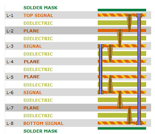
“This design could easily be redefined as an eight-layer, 2-4-2 HDI board with two sequential laminations,” Atar concluded. “All drill to copper criticality would vanish with the HDI architecture. Traces can be healthy 4 mils to 5 mils, or even wider because no traces have to be threaded between adjacent vias in pads.”
If the customer had created the layout on the stack-up shown in Figure 1, boards could easily be manufactured with excellent yield and four fewer layers. The exercise consumed very little time.
Don’t travel alone and head down a one-way street with no return. Ask for a little help before the journey and you’ll have a great trip.
Also read: 9 HDI Considerations for Manufacturability and Cost
Yield drives profit
The first step toward designing a printed circuit board is to identify the least expensive materials that satisfy the electrical and environmental requirements of the application. Datasheets and price lists for materials provide basic guidance but offer no clue about how much the board would actually cost to fabricate using one material versus another. Often, data sheets will show two materials to have nearly identical characteristics, but one may be relatively more or less challenging to process than another, especially for HDI technology. Their raw prices have little correlation to their ease of manufacture and consequently to board yield, and it is the manufacturing yield that drives profits.
Consult your board manufacturer at the outset of design to identify materials that would provide the optimum balance of price, manufacturability, and performance based on your construction.
Broadly, the manufacturing yields of HDI designs for which material is specified are determined by whether the material is dimensionally stable, susceptible to or resistant to copper migration such as conductive anodic filament (CAF) growth, able to withstand multiple laminations, and able to be laser drilled with consistently good results.
A circuit whose response remains relatively flat over its frequency range will faithfully propagate signals without distortion. The dielectric constant (Dk or Er) of a material decreases as frequency increases. High-speed digital signals involve broad bands of frequencies and thereby are subject to distortion caused by impedance variations resulting from changes in the Dk of board materials with frequency. Changes in the dissipation factor (Df) of board materials with frequency degrades signal integrity as well. Materials whose Dk and Df are low and vary little across the frequency domain of a circuit propagate signals faster and maintain signal integrity better than materials with higher Dk and Df.
Suppose you’ve ruled out dielectrics in the FR-4 category because their Dk and Df values are too high and vary too much over the signal spectrum of your circuit. Suppose as well that your board will incorporate several high-speed devices in BGAs, each with a dense pin matrix that will require via-in-pad routing. Your design will therefore involve blind microvias and require a material thin enough that the aspect ratio of those laser-drilled vias does not exceed 0.8:1 or else the plating could become difficult to achieve. Remember, at a given Dk, the thinner the substrate, the narrower the traces must be to maintain a 50-ohm impedance. You’ll favor materials that have a low Dk so trace width can be wide enough to be easily manufactured and provide the necessary impedance value.
Comparing Isola FR408HR, Nelco N4000-13 SI, and Panasonic Megtron 6
Let’s say a Dk under 3.7 at 1GHz is acceptable and you’ve decided Isola FR408HR, Nelco N4000-13 SI, and Panasonic Megtron 6 are prospects, based on their datasheets. We chose these three materials, which our fabrication company deals with routinely, to illustrate our point about hidden manufacturing issues, yield, and ultimate HDI PCB cost.
FR408HR has a higher dielectric constant and higher loss factor than both N4000-13 SI and Megtron 6, but it is cheaper in price. The Nelco 4000-13 series of materials, and in particular N4000-13 SI, have excellent electrical properties for high-speed digital applications. The SI (signal integrity) material is based on a glass cloth specially formulated to have a very low Dk over a wide frequency range that is closely matched to the Dk of its resin. Megtron 6 incorporates a unique low-Dk fabric known as flat glass. Unlike FR408HR and N4000-13 SI, in which resin resides throughout the glass fabric weave, its resin is essentially a “butter coat” evenly distributed across the woven flat-glass fabric surface. Megtron 6 has a slightly higher average Dk value than Nelco 4000-13 SI, from 1GHz to 10GHz, but a much lower Df. It is somewhat more expensive than the Nelco material and is often used for RF and microwave applications, as well as for high-speed digital circuits.
The three products are comparable on paper (all are widely employed for high-speed digital PCBs), but they have quite different manufacturing characteristics when used for HDI board designs.
Three important factors that influence HDI PCB fabrication
There are three key qualities a material must possess for HDI fabrication. First, it must be dimensionally stable, a quality that, of course, applies to non-HDI construction as well. All materials shrink and stretch to some extent during manufacturing processes, and patterning must be scaled to compensate, which is not an issue provided the material movement is predictable. Second, the material must be easily machinable: For HDI that means it can be laser drilled without problems. Third, a material must be able to survive multiple laminations. Let’s restrict this comparison of manufacturability to laser drilling, with regard to the three materials.
The word drill is really a misnomer to describe how a laser makes holes. A better term would be vaporization. Highly concentrated energy is directed in a focused beam on a specific area, which is absorbed by the material until it vaporizes. The energy must be carefully controlled to ablate material to form a hole without destroying the landing pad beneath. However, dielectric constituents absorb energy at different rates, and it is in this respect that N4000-13 SI, FR408HR, and Megtron 6 differ in manufacturability.

How to choose the right resin?
Epoxy resin is the most commonly used thermosetting resin and is the backbone of the industry. Thanks to its relatively low cost, excellent adhesion (to the metal foils as well as to itself), and good thermal, mechanical, and electrical properties. Epoxies are thermosetting resins that use catalysts and hardeners to increase the adhesive properties.
Epoxies are flammable material. Since the modern high-density circuit board dissipates more heat, flame retardants are incorporated into the epoxy to reduce flammability. But retardants are not useful in the case of organic chip packages, marine and industrial environments where higher thermal stability is required.
BT-Epoxy (Bismaleimide-Triazine Epoxy) is used in organic chip packages. Polyimide and Cyanate ester resins are used for better electrical properties along with thermal stability. Compared to the epoxy resin these are expensive.
Polyimide and Polytetrafluoroethylene (PTFE) are thermoplastic resins-variants used for flexible and rigid-flex PCBs., They are suitable for high-frequency and wireless applications because they have excellent electrical properties and low absorption of moisture.
Type of via influences the HDI board cost
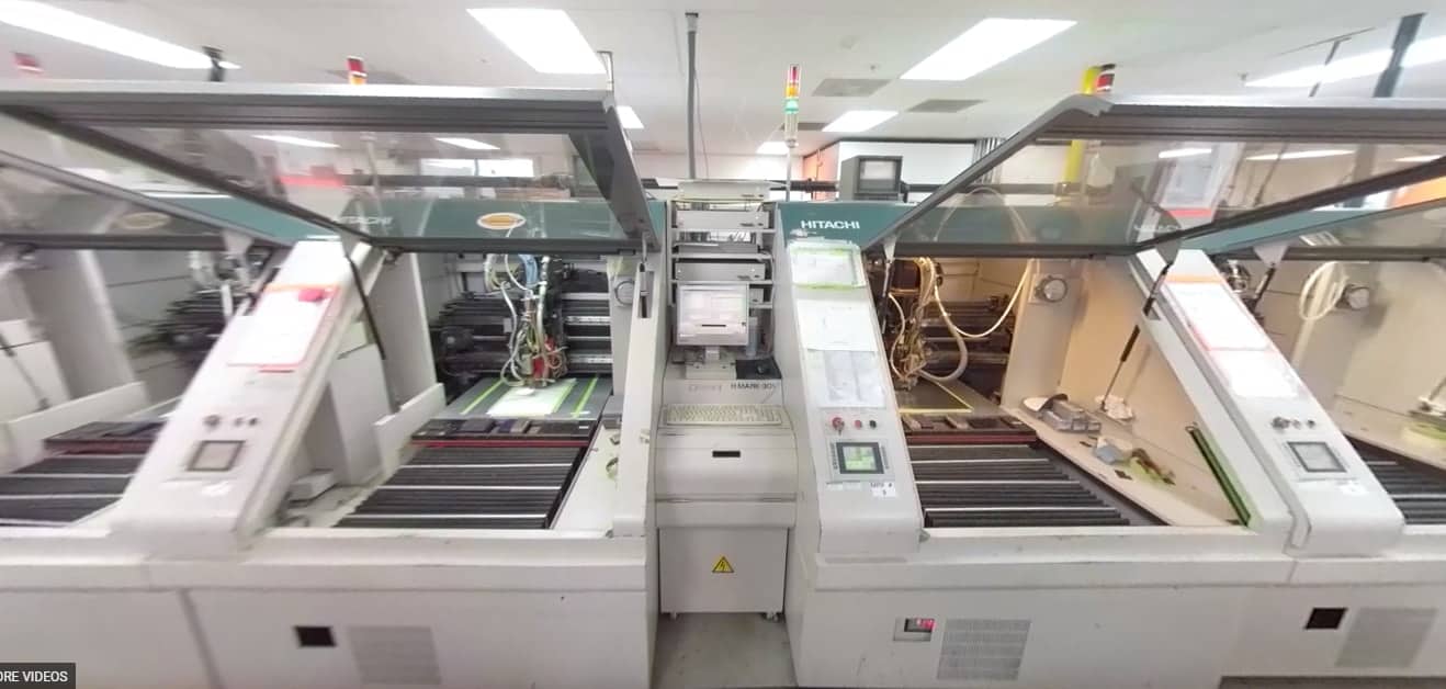
The via quality and plating of an HDI PCB has a direct relationship with the end product quality and HDI PCB cost. Mechanical drilling and laser drillings are the most commonly used via drilling formats. Mechanical drilling is the conventional drilling technique, which is still used as an efficient drilling method for through-hole vias and blind vias since it is economical.
If mechanical drills are used for drilling in HDI PCBs, high-speed spindles are combined with different kinds of depth sensors. The precise production of blind vias requires special techniques like drill depth control to ensure repeatable blind via formation.
The capital cost for mechanical drills is low compared to laser drilling. But it is not the same in case of operational cost. Also, a broken drill hole costs extra as it requires extra metallization and additional operating charge as well. So, for critical drilling and large-scale production laser drilling is preferred.
If we are comparing the cost of drilling one via, mechanical drilling is economic compared to laser drilling. But if we are considering the cost of 1000 vias with high precision, consistency of drill quality, and high-speed processing, laser drilling is economical. Choosing the right drilling technology is one of the crucial factors for optimizing the HDI PCB cost.
Laser direct imaging (LDI)
LDI is a method of imaging circuitry patterns directly on the PCB without the use of a phototool.
- Cost-saving from eliminating conventional phototools
- Elimination of film-related and printed-in defects which seeks rework
- Saving cost by minimizing time to set-up print and other jobs
- Enables flexible manufacturing route.
The importance of communicating with PCB manufacturers
Let us interject a disclaimer: Though our company has extensive experience with the three materials, that experience isn’t quantified and therefore must be considered subjective. There’s no bias toward one rather than the others, except for HDI from manufacturing experience. We’ll build whatever a customer wants if it can be constructed. The point to bear in mind is simply this: If a board is challenging to build in limited, prototype quantities, it will be no less challenging to manufacture in production runs. To repeat, yield drives profit.
Our company, Sierra Circuits, has found that achieving clean laser-drilled holes in the Nelco material and in FR408HR requires more effort compared to creating them in Megtron 6. The resin in the Nelco fabric burns off at a much different rate than the glass fibers and too much energy is required to consume all the fibers in the hole without compromising the surrounding dielectric and the landing pad itself. FR408HR is less prone to have glass fibers protrude from hole walls than is N4000-13 SI but is less predictable in that respect. Glass bundles extend in perhaps only 5% of the holes but such inconsistency itself complicates processing. The flat glass fabric of Megtron 6 can be ablated cleanly by contrast to the other two materials, in our experience.
Nelco is continually investigating resin formulations, glass, and fabric constructions that would improve the manufacture of HDI architectures. The firm recently introduced a new material, N4800-20 SI, which it recommends in place of N4000-13 SI for HDI PCB manufacture. Our company is evaluating that material and anticipates better results.
To summarise, in order to get the optimal HDI PCB cost, one has to consider several factors such as yield, material type, via drilling methods, and imaging. The advantage of HDI is higher yield due to better control of drill to copper and use of traces above 3 mils. HDI also results in a lesser number of PCB layers.
The upshot of all this is that you should consult your board manufacturer at the outset of design to identify materials that would provide the optimum balance of price, manufacturability, and performance based on your construction. We’ll dedicate this column as the first installment regarding materials and manufacturability. The next one will regard materials with the highest electrical performance for digital high-speed circuits, and for RF and microwave applications.

HDI PCB Design Guide
5 Chapters - 52 Pages - 60 Minute ReadWhat's Inside:
- Planning your stack-up and microvia structure
- Choosing the right materials
- Signal integrity and controlled impedance in HDI
- Manufacturing considerations for higher yields
Download Now
About Amit Bahl : Amit Bahl, widely recognized as the PCB Guy, earned his Bachelor of Science in Engineering from UCLA. He is currently the Chief Revenue Officer at Sierra Circuits, where he continues to lead efforts to simplify the PCB design journey and support designers and engineers in creating high-quality boards.