Contents
Design for manufacturing (DFM) guidelines resolve potential issues that can occur during the manufacturing and assembly of circuit boards. DFM for flex and rigid-flex PCBs with SMT involves selecting application-specific circuit construction types, laminates, coating thickness, trace routing strategies, bending, and EMI capabilities.

What are the DFM guidelines for flexible and rigid-flex circuits?
DFM for flex and rigid-flex PCBs are categorized as given below:
- Establishing flex circuit construction types
- Base materials
- Cover coating and film variations
- Conductor routing and physical feature planning
- Flexible circuit bending and folding guidelines
- EMI shielding and impedance control methodology

Establishing flex circuit construction types
Flex boards are classified into single-sided, double-sided, multi-layered, and rigid-flex boards.
IPC type 1- Single-sided flex boards
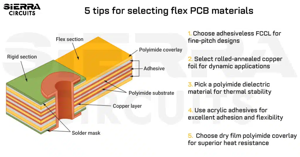
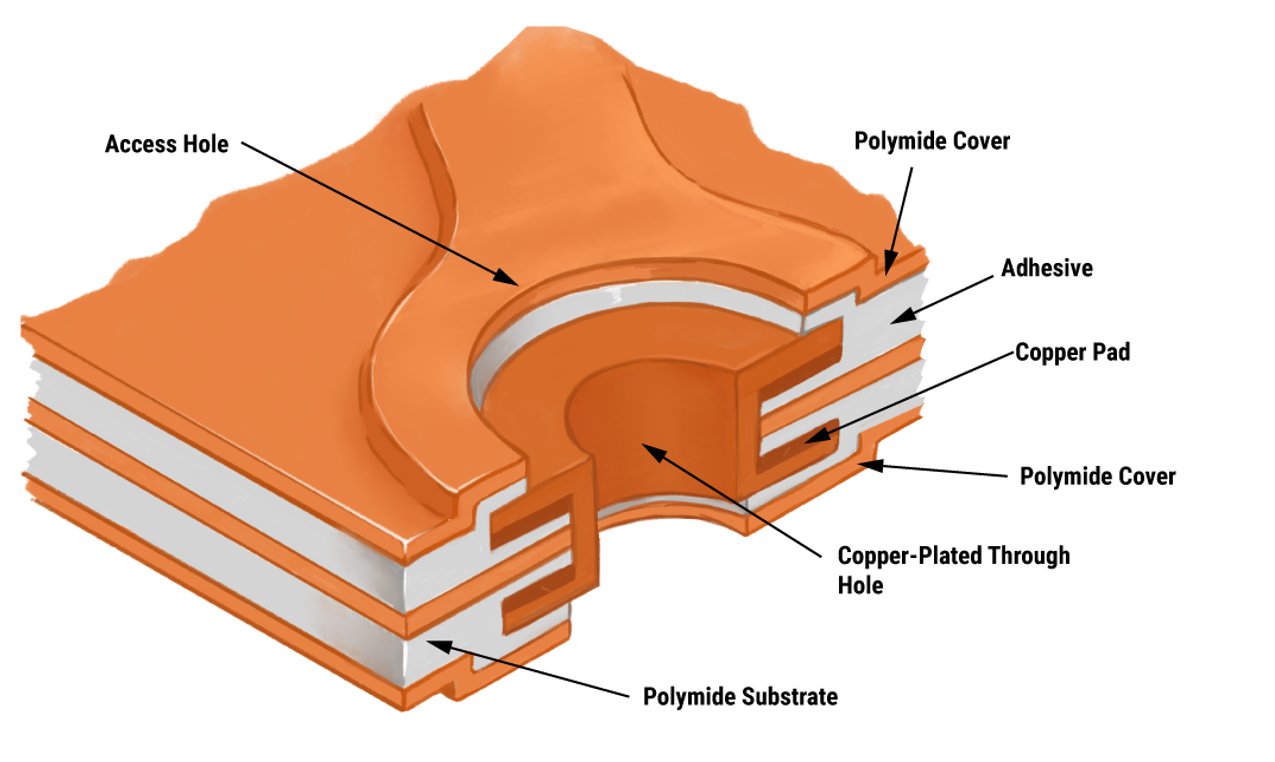
Single-sided boards are the most common type. These PCBs consist of a single conducting layer bonded onto a dielectric base film. Generally, it includes an insulating layer to protect the conductor pattern. A polyimide coverlay can be used for the insulation and environmental protection of the circuit. SMT lands (surface mount land sockets) are accessible only from one side when they are provided. Single metal flexible circuits are perfect for dynamic applications.
IPC type 2- Double-sided flex boards
IPC type-2 flex PCBs consist of two copper conductive layers and a flexible dielectric film material that serves as an insulator between them. The copper foil is bonded or deposited onto both sides of the base dielectric film.
Cu-plated through-holes that extend through the flexible material complete the interface between the circuit layers. The circuit pattern is imaged, chemically etched, and finally insulated on both sides by applying a top and bottom dielectric cover-layer or cover-coat.
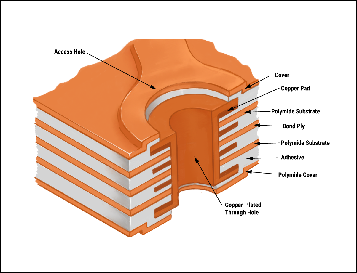
IPC type 3: Multi-layer flexible boards
Multi-layer flex circuit boards consist of three or more conductive layers bonded together with a dielectric. Interconnection between conductive layers is provided by plated through-holes. By using multilayer boards, designers can overcome certain challenges like crosstalk, unavoidable crossovers, specific impedance requirements, and dense component layouts.
IPC type 4: Rigid-flex circuit
A rigid-flex circuit combines epoxy glass reinforced material and flexible film with copper circuit patterns interconnected with plated through holes. This configuration provides flexibility in a certain portions of the board while using rigid portions for mounting and interconnecting components in the rest of the circuit design.
To learn about the potential DFM errors in rigid-flex PCBs, see 13 common DFM mistakes in rigid-flex PCBs and techniques to avoid them.
What are the base materials for flexible and rigid-flex circuits?
Usually, substrates for rigid-flex circuits are developed using processes similar to conventional board fabrication. A detailed description of the specification for glass-reinforced and non-reinforced base materials can be found in IPC-4101 through IPC-4104. Some of the base materials include:
- Polyimide film
- Polyimide with glass fiber reinforcement
- FR-4 epoxy with glass fiber reinforcement
- BT-epoxy with glass fiber reinforcement
Flex PCB Design Guide
10 Chapters - 39 Pages - 45 Minute ReadWhat's Inside:
- Calculating the bend radius
- Annular ring and via specifications
- Build your flex stack-up
- Controlled impedance for flex
- The fab and drawing requirements
Download Now
Base material properties
It is important to choose the product that best suits the design. The following chart shows the classification of materials according to the key attributes.
| Key attributes | Polyimide film | Polyimide laminate | FR-4 laminate | B-T laminate |
|---|---|---|---|---|
| Glass transition temperature (Tg) | 341℃ | 265℃ | 170℃ | 190℃ |
| Decomposition temperature (Td) | N/A | N/A | 340℃ | N/A |
| Reinforcement type | None | E-glass | E-glass | E-glass |
| Dielectric compound | Polyimide | Polyimide | Epoxy | (Note 1) |
| Maximum operating temperature | 225℃ | 230℃ | 150℃ | 200℃ |
| Moisture absorption | >1.0% | 1.0% | 0.5% | 0.35% |
- B-T laminate material is a mixture of epoxy and bismaleimide-triazine resins.
- The FR-4 material conforms to IPC-4101/126, 129,130, and 131. It is developed for Pb-free solder processing (240℃-260℃).
DFM for flex and rigid-flex PCB material
Below are the parameters that should be considered while choosing materials that meet the design criteria:
- Moisture absorption
- Fire retarding
- Electrical properties
- Mechanical properties
- Thermal properties
See our post, how to choose PCB materials and laminates for fabrication to gain a better understanding of material characteristics and selection attributes.
Key physical attributes for polyimide film dielectrics
- Outstanding electrical properties
- Excellent chemical resistance
- Thermally stable, capable of continuous operation at a temperature >225ºC
- Dimensionally stable at high or low temperature
- Able to withstand process temperatures for SMT soldering
Polyimide film dielectrics are expensive but suitable for a variety of electronic applications.
Surface protection for flexible circuits
For flexible circuits, surface protection is essential to prevent them from getting affected by environmental hazards. The surface of the board is protected using coverlay, covercoat, liquid photo-imaged polymer, and photo-imaged dry film.
- Coverlay– Coverlay is a dielectric film applied on the circuit pattern with an adhesive.
| Advantages of coverlay | Disadvantages |
|---|---|
| Excellent dynamic flexibility | Thickness and cost increase depending upon the application |
| Pinhole free | Requires precutting and pre-punching operations |
| Highest dielectric strength | Susceptible to mis-registration/dimensional change |
- Covercoat– Covercoat is a liquid polymer screen printed onto the circuit board and cured using UV light or heat.
- Liquid photo-imaged polymer– It is a photosensitive polymer spray, printed or flooded onto the board and photo-imaged to provide access to land pattern features.
| Advantages liquid photo-imaged polymer | Disadvantages |
|---|---|
| High pattern resolution | Flexibility varies by supplier |
| Eliminates punching and drilling of access holes | Moderate cost, minimal material waste |
| Enables precise alignment for exposed features | If very thin, pinholes may form in coating |
- Photo-imaged dry film– Fusion laminated onto circuit and photo-imaged to provide access to land pattern features.
| Advantages photo-imaged dry film | Disadvantages |
|---|---|
| High pattern resolution | Flexibility varies by supplier |
| Eliminates punching and drilling of access holes | Basic material cost is high but material is pinhole free |
Flex and rigid-flex fabrication process limitations designers need to know
Some factors that will define the supplier’s fabrication capabilities include:
- Minimum distance separating conductors, vias, though-holes, and SMT land patterns.
- The maximum number of conductors routed between a given area or fixed surface features.
- The number of conductor layers required for flexible and rigid portions of the circuit.
Parallel circuit routing variations
In parallel circuits, the conductor path on the flex board must change the direction. The designer should avoid sharp 90° turns. Ideally, the conductor path should be designed with a nested, chamfered, or generous radius. The multiple conductor path routed in parallel should also maintain uniform spacing with a progressive, larger radius from the center axis.
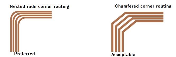
In parallel circuit routing, it is necessary to make sure that sharp corners are not present that promote tearing. The figure shown below represents the key features that will enhance the survivability of flex circuits.
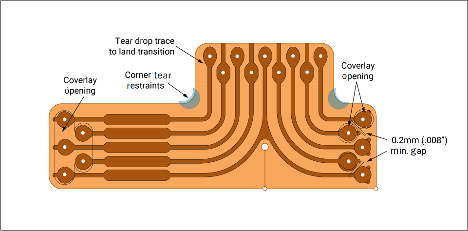
It is possible to reinforce the interface using a simple teardrop shape transition between narrow and wide conductors. For holes furnished for mounting pinhole components, it is good design practice to make the mounting pad area as large as possible to maximize the adhesion area during PCB soldering.
Circuit routing and spacing
Determining conductor density in routing will depend upon the number and width of signal conductors. For single and double-sided flex boards, the overall width of the base material should provide adequate surface area for coverlay film bonding. The base material also provides sufficient spacing for bonding. The table given below classifies trace width and spacing criteria based on the copper foil thickness.
| Copper foil thickness | 1/2 OZ | 3/4 OZ | 1 OZ |
|---|---|---|---|
| Dimension | 17µm | 26µm | 34µm |
| A | 0.13mm | 0.19mm | 0.25mm |
| B | 0.13mm | 0.19mm | 0.25mm |
| C | 0.75mm | 0.75mm | 0.75mm |
| D | 0.50mm | 0.50mm | 0.50mm |
See our case study, routing microcontroller and BGA in rigid-flex PCBs to learn strategies we implemented to accurately fanout small-pitch BGA and microcontroller.
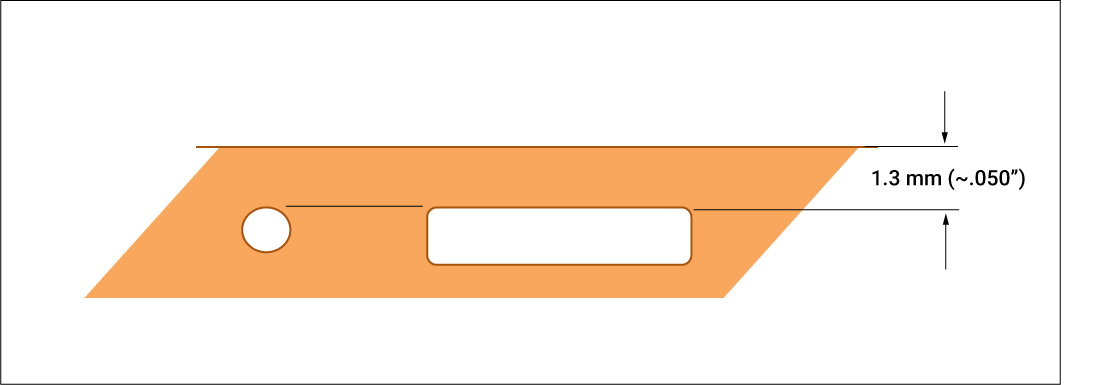
Hole-to-edge clearance guidelines
The minimum distance between the exterior edge of the flex circuit outline and the edges of interior holes and cut-outs should not be less than 1.3mm. The larger the hole-to-edge distance, the more reliable will be the part.
Tear avoidance guidelines
The IPC-2223 section is a design standard that makes recommendations for flex and rigid-flex circuits. The corners should be about 1.5mm wide. However, larger radii will make a more reliable part and thus minimize tearing. In the following image, we can see chamfers, relief, and radius on the corners. Tear restraints give a little more strength to the corners to avoid tearing when the material stretches. Even though the material is hard, it will tear if stretched beyond its limit.
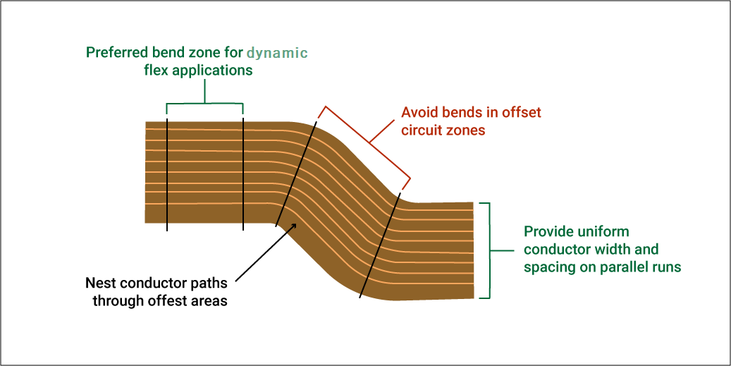
Conductor routing in bend zones
While routing conductor in bend areas consider the following:
- The conductor should be routed perpendicular to the bend area.
- It should be evenly spaced across the bend zone.
- Do not apply additional metals in the bend area.
- The conductor should maintain uniform width.
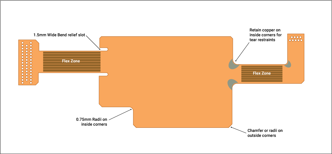
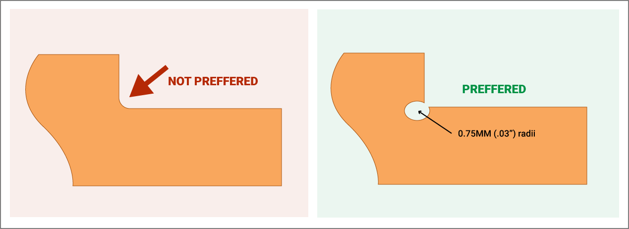
How to avoid 90° inside corner in flexible sections
While dealing with corners, it is necessary to avoid 90° inside corners to prevent tearing. The minimum radius profile should be 0.75 mm to reduce cracking on the inside corners of the flex film. However, larger radii or recessed radii will make the corner more resistant to tearing.
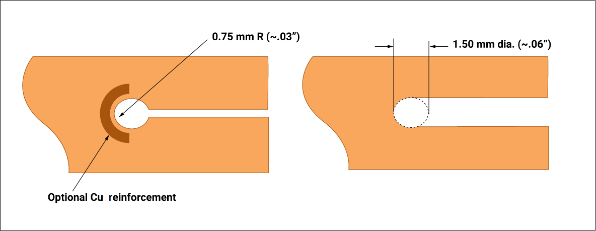
Tear restraint for narrow slot features
If the circuit area is subjected to repeated flexing, it is recommended to retain a small pattern of copper foil for further reinforcement against tearing. The slot features should have 0.75mm radii.
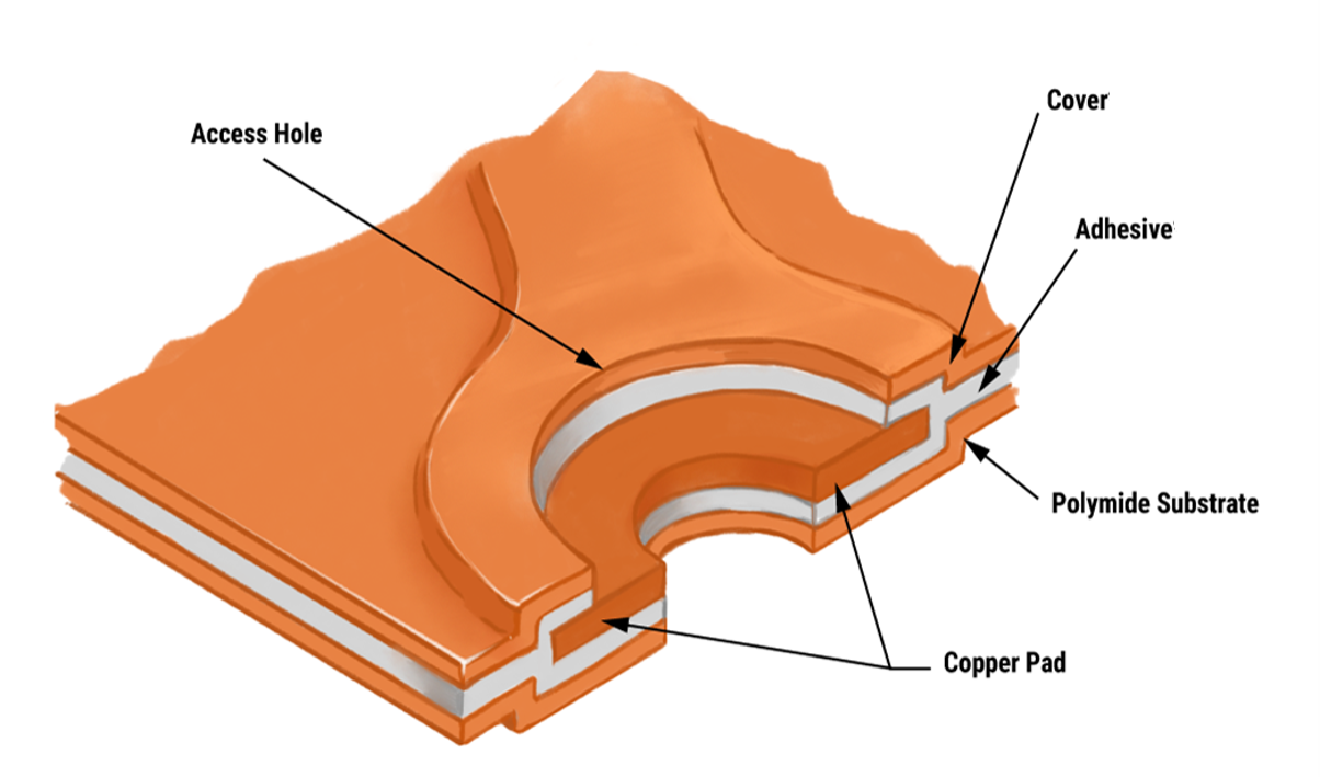
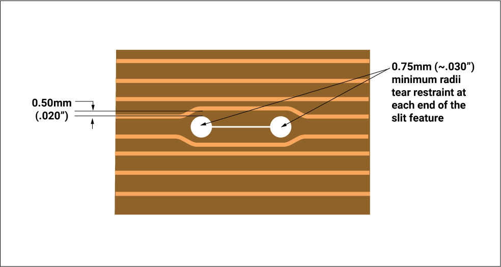
Incorporating slit features within the circuit
The image shown below exhibits a narrow slot that represents minimum clearance from the hole (0.50mm).
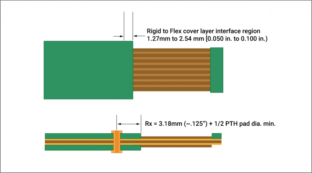
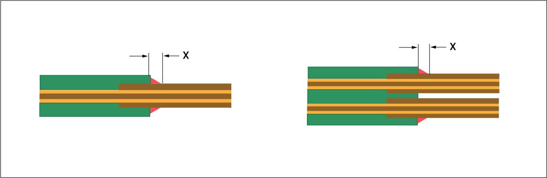
Strain relief fillet for rigid-to-flex transition
A small bead of polymer is applied at the transition of the flexible and rigid section to minimize physical stress at the interface. The strain relief material can be a flexible epoxy, acrylic, RTV silicone, polysulfide compound, etc.
The strain relief horizontal dimension (X) may range between 1.0mm and 2.5mm [~0.0394in. to ~0.0984in.].
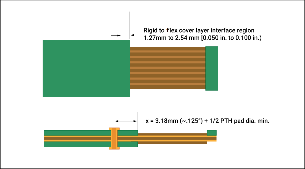
Flex-to-rigid conductor interface
To avoid compromising the integrity of plated through-hole on the rigid-flex circuit, the hole locations must be set back from the edge of the rigid sections. Here, 3.18mm + ½ PTH pad diameter is a setback that will avoid interference from the cover layer protrusions where flex material enters rigid-flex material. This is one of the most important considerations when it comes to DFM for rigid-flex PCBs.
To learn more about how to overcome reliability issues in rigid-flex designs, see air gap construction method in rigid-flex PCBs.
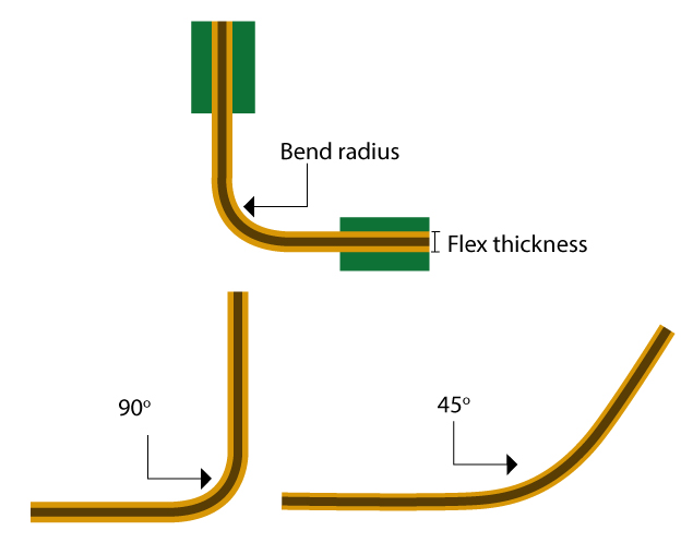
Bend and fold guidelines for static applications
The minimum bending radius for 90° bend-to-install depends upon the number of copper layers. Generally accepted guidelines are:
- Single-sided – 10:1
- Double-sided – 10:1
- Multilayer – 20:1
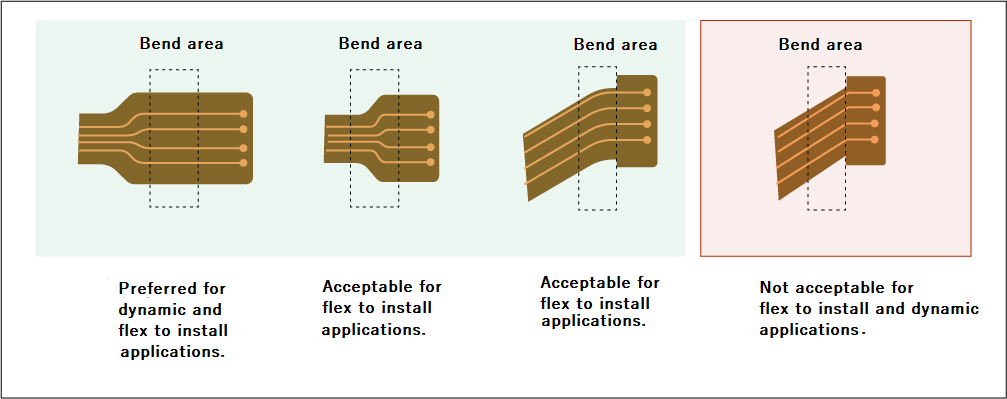
Conductor routing dos and don’ts in the bend area
For proper conductor routing, it is essential to know the dos and don’ts. Refer to the image below:
Folding flex circuits
In folding flex circuits, copper conductors in the fold area should always be on the inside surface of the fold. These folds are preferred for one-time folding on single-sided flex circuits. If the copper foil is on two sides of the flexible circuit, copper on the outside area must be cleared.
90° or greater fold-to-install
Folds are preferred only for single or double-sided flex circuits. Folds should be uniform and designed to follow the surface of the package. To control the bend radius and prevent conductor cracking, a forming tool might be used.
A crease may be formed only once and then bonded into place, ensuring that the fold will not be exercised.
Bend guidelines for dynamic applications
The recommended minimum bending radius for dynamic applications that require repeated bending up to 90° is:
- For single-sided flex, 100:1
- For double-sided flex, 150:1
However, multilayer dynamic flexing is not recommended.
Two-sided flex circuit bend zone
The following image shows dos and don’ts for copper conductor routing in double-sided flex circuits.
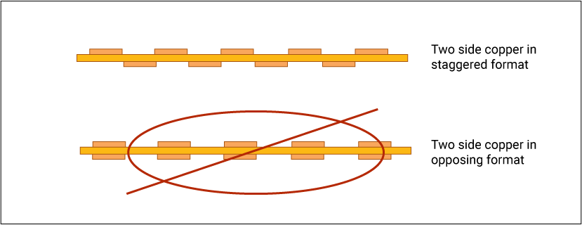
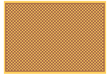
EMI shielding and impedance control for two Copper layer flex
A patterned conductive layer may be added to provide an effective EMI shield. The crosshatched pattern helps to maintain flexibility.
Fabricators and designers should understand the requirements for limiting signal loss, impedance tolerance, and electromagnetic interference (EMI).
Watch the whole webinar to get a proper understanding of the following points:
- DFM for flex and rigid-flex PCBs.
- SMT component selection and land pattern development
- DFM for SMT assembly processing
Choosing an appropriate IPC construction type based on flex and rigid-flex application requirements is the first step in the DFM process. It is crucial to adhere to specific design for manufacturing guidelines as it can eradicate issues related to trace routing, spacing, clearance, conductor interface, etc.
If you want to learn more about any critical aspect of flex boards, then let us know in the comment section.

Design for Manufacturing Handbook
11 Chapters - 96 Pages - 90 Minute ReadWhat's Inside:
- Annular rings: avoid drill breakouts
- Vias: optimize your design
- Trace width and space: follow the best practices
- Solder mask and silkscreen: get the must-knows
Download Now