


Contents
When routing microcontrollers and BGAs, you need to consider the trace spacing requirements of your design and clearance between the pins. Techniques such as via-in-pad, staggered vias, and dog-bone routing enable you to efficiently fan out pins of low-pitch devices.
In this case study, you’ll learn:
- How we used via-in-pad technology to break out the inner pins of a BGA and a microcontroller on a medical rigid-flex PCB.
Client’s design specifications for rigid-flex medtech PCB
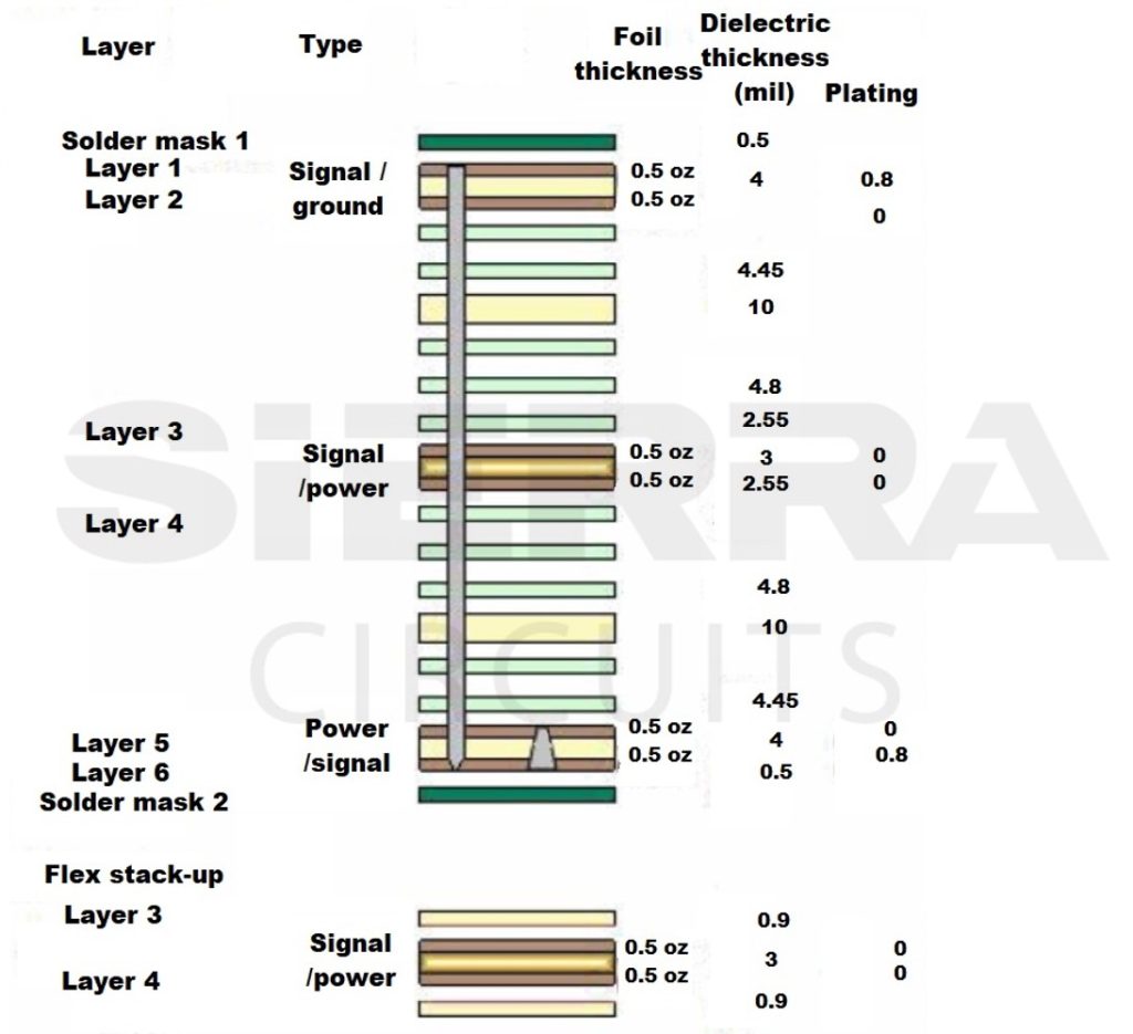
- This is a 6-layer rigid-flex board where layers 3 and 4 are flex sections.
- FR370HR and Arlon 38N are used to build the rigid and flex parts, respectively.
- The circuit requires 90Ω controlled impedance with ±10% tolerance.
- The operating frequency is set at 64 MHz and the maximum working current is 1 amp.
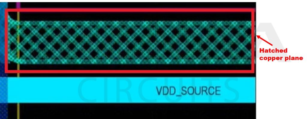
- To provide mechanical support to the flex section, we incorporate copper hatching instead of a standard copper plane.
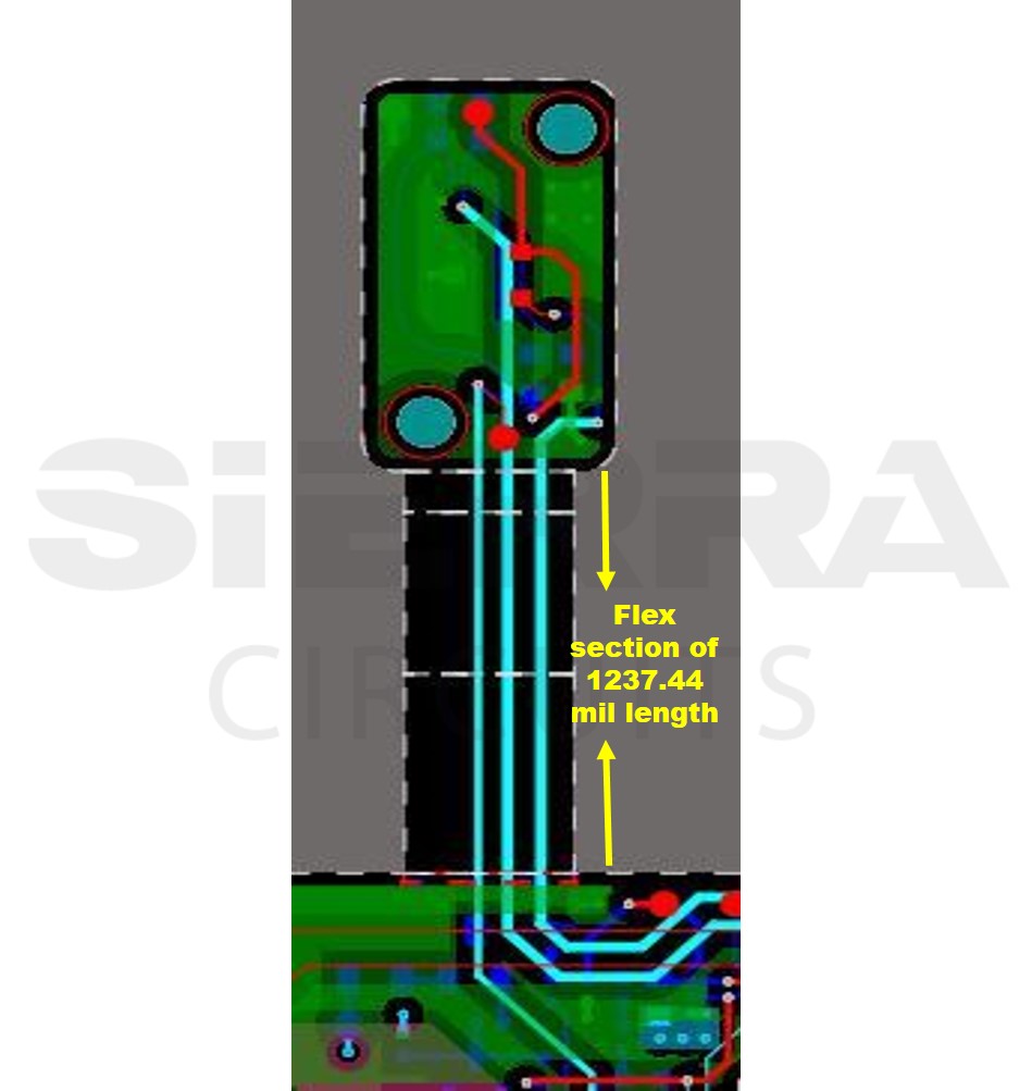
- The design has 3 flex sections with lengths of 1237.44, 646.88, and 595.59 mil.
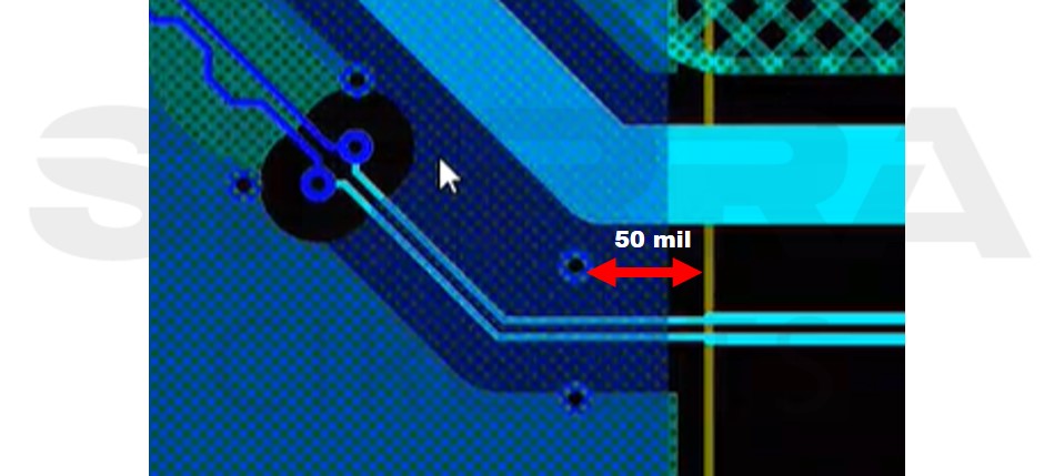
- The clearance between flex edges and vias should be 50 mil to prevent signal loss.
- The design has an nRF5340 microcontroller with 0.4 mm (16 mil) pitch. It has a clock frequency of 64 MHz. Moreover, this high-speed SOC processor includes 256 KB flash and 64 KB RAM.
- This circuit includes an LED and a motor controller.
- 2.06 GHz USB-C interface offers 10 Gbps data transfer and 100 watts of power in the circuit board.
- Lithium-ion rechargeable battery with a long lifespan and high energy density.
- The watchdog timer (WDT) in the circuit should reset the microcontroller after a specific time interval and prevents any malfunctions.
- 0.4 mm BGA
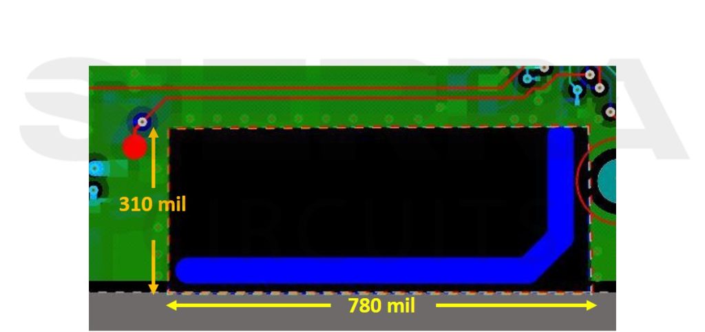
- An RF antenna of a cross-section of 780 ✖ 310 mil is incorporated to facilitate Bluetooth communication in the circuit. The antenna does not have any copper features around it to prevent EMI and crosstalk.
To learn the essentials of designing a PCB antenna, watch our interview on best practices for designing PCB antennas for wireless applications.

Challenges in routing the microcontroller and BGA on this rigid-flex board
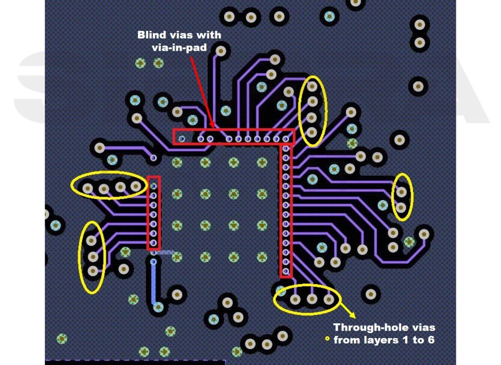
Breaking out the inner pins of the microcontroller
As a good design practice, maintain 4.25 mil spacing on both sides of a 4 mil trace for a 0.5 oz copper weight. The air gap between the inner pins of the microcontroller is 6.89 mil. Therefore, in this board, we do not have sufficient space to breakout the inner pins of the processor.
Resolution
To resolve this issue, we implemented a blind via from layer 6 to layer 5 using the via-in-pad technique. In addition to this, we placed a track on layer 5 and connected it to the through-hole. This enabled us to fan out the inner pins of the microcontroller.
To learn how we resolved the challenges in designing microcontrollers and functional PCBs with antenna signals, see our case study, designing microcontroller and functional PCBs with an antenna.
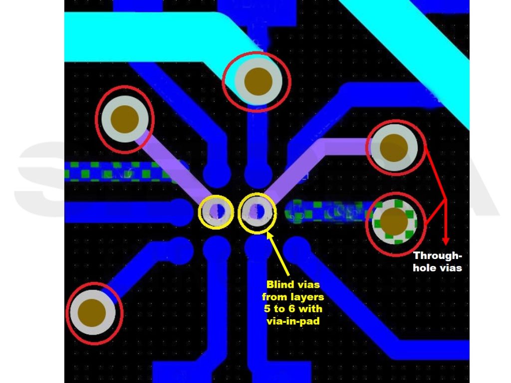
Routing the center pins of the 0.4 mm BGA
It was difficult to route the center pins of the BGA with 4.25 mil clearance as the air gap between the pins is 5.75 mil.

Resolution
We overcame this challenge by drilling via-in-pad through the center pins. To achieve a 0.8 aspect ratio for the blind microvias, the drill size was kept at 6 mil for a 12 mil pad and dielectric thickness of 4 mil. Moreover, we filled these blind vias with conductive material to ensure the correct board connectivity.
Key takeaways:
- Incorporate via-in-pad technique to achieve the correct fanout for routing small-pitch BGAs and microcontrollers.
- Always fill the vias with conductive or non-conductive material if your design has a via-in-pad.
- Optimize the drill size as per the dielectric thickness to attain the correct aspect ratio.
Flex PCB Design Guide
10 Chapters - 39 Pages - 45 Minute ReadWhat's Inside:
- Calculating the bend radius
- Annular ring and via specifications
- Build your flex stack-up
- Controlled impedance for flex
- The fab and drawing requirements
Download Now
Discover how we handled the challenges of designing a rigid-flex video board in our case study: design of a rigid-flex video board.
Our PCB designers analyzed the trace clearance and width with the respective copper weights during the design phase. Subsequently, they set the required design constraints and incorporated the via-in-pad technique to achieve an efficient fanout for routing BGA and microcontroller present in this rigid-flex medtech PCB.
While designing a rigid-flex board, it is vital to adhere to IPC-2223 regulations to optimize the bending performance and eliminate manufacturing errors. If you require any assistance in designing your rigid-flex board, please comment below. Our design and manufacturing experts will be happy to help you.
About Poulomi Ghosh : Poulomi is a microwave engineer specializing in EMI, EMC, RF, and high-speed electronics. As a senior technical writer at Sierra Circuits, she creates advanced engineering articles and webinars for hardware engineers and PCB designers.


