


Contents
Common DFM mistakes in rigid-flex include wrong choice of dielectric materials, misplacing the through-holes, insufficient bend radius, unoptimized stack-up, and inadequate spacing between the conductors.
Highlights:
- DFM errors in rigid-flex designs cause production delays, increased costs, and lower product quality.
- Steps to design the most cost-efficient rigid-flex PCB using Altium Designer.
- Things to include in your rigid-flex fab notes.
Before we dive into the comprehensive guide on the common DFM pitfalls in rigid-flex PCBs, take a quick look at these essential tips to ensure your board design is on the right track.
Catch valuable insights on common rigid-flex DFM mistakes and best practices for designing rigid-flex PCBs in this webinar, and read on for a comprehensive summary of the key takeaways.
Click here to watch the whole DFM: Rigid-flex webinar.
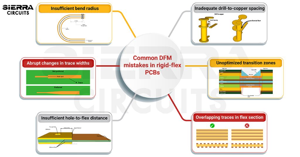
13 DFM mistakes in rigid-flex PCB
If you intend to develop a rigid-flex PCB for your specific aerospace or medical application, it is imperative to adhere to a set of DFM rules that will not only ensure the success of your project but also prevent the occurrence of potentially expensive errors. Here are some of the common DFM mistakes to avoid when designing rigid-flex PCBs.
1. Unfavorable rigid-flex PCB material selection
Choosing the right dielectric materials is crucial to ensuring durability, performance, and reliability in your rigid-flex PCBs. Standard prepreg with high resin content is not suitable for rigid-flex PCBs, as the excess resin will run onto the flexible section, hardening and rendering them inflexible.
Here are some material selection tips:
- Use no-flow or low-flow prepreg such as 1080 and 106 glass fabrics.
- Use at least 3 layers of prepregs to ensure a strong bond between the layers. If you employ just one layer, there are chances of air gap creation leading to high-resistance shorts.
- For the flex sections, either use adhesiveless cores.

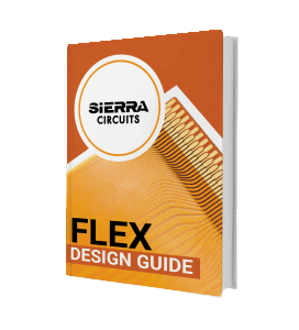
PCB Material Design Guide
9 Chapters - 30 Pages - 40 Minute ReadWhat's Inside:
- Basic properties of the dielectric material to be considered
- Signal loss in PCB substrates
- Copper foil selection
- Key considerations for choosing PCB materials
Download Now
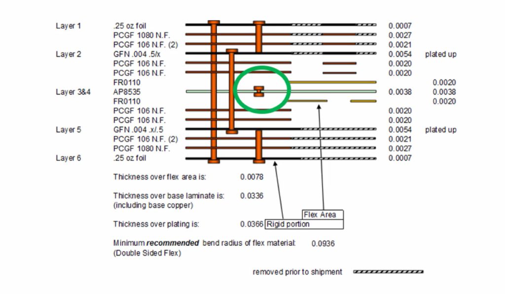
2. Unoptimized stack-up and via placement
Stack-up is the foundation of a robust rigid-flex board. It directly impacts the signal integrity and mechanical stability of your design. Designing an optimal layer stack is a critical step in ensuring the design’s success.

To design an efficient rigid-flex build-up stick to the following design guidelines:
- Do not place the flex layers on the outer layer of the board. Always place them at the center.
- Maintain symmetry and balance in both copper distribution and dielectric materials.
- Pair signal layers with reference planes to minimize signal coupling and control impedance in flex sections.
- Have an even number of layers to prevent slipping and warpage.
- Each layer in your build-up should include a clear description of the thickness and impedance requirements.
- Employ the bookbinding technique to enable multilayer flex bends without experiencing deformation. This involves manufacturing the layers in increasingly longer lengths along the outer bend radius.
- Maintain uniform finished thickness for rigid parts to avoid the need for extra lamination operations for separate rigid parts with different board thicknesses.
- Minimize the use of vias in the flexible areas. You must position vias at least 20 mil from the rigid-flex/flex interface.
Also read, 7 must know for your first flex PCB design.
How to rightly place flex layers and vias on your rigid-flex stack-up
The stack-up below shows a 3-layer stack-up with the flex layer on the outside. This configuration is manufacturable, however, it comes with some difficulties. The flex layer has some traces that cross over low-pressure areas during manufacturing which makes the surface uneven due to the cavity, making imaging, etching, and plating more difficult.

Instead, you can position the flex layer in the center of the stack-up as shown in the image below. In this case, the flex layer is covered with the rigid layer throughout the manufacturing process, with the rigid portion being removed at the end to expose the flex.

Here’s an example of less preferable via placement in a layer stack.
Placing the vias in the flex area for connection makes the manufacturing costlier. Always place the vias in a rigid area (as shown below) to increase the reliability of your design.
3. Improper routing across the bending area
Improper routing can result in reliability and signal integrity issues. Consider these guidelines when you route your next rigid-flex design:
- When you’re routing signals on bend areas, ensure they’re kept as straight, perpendicular lines, and try not to make any sharp turns.
- If the traces on a flex area need to change direction, use curves rather than 45° or 90° corners.
- When working with a flexible surface, it is preferable to use narrower and uniformly spaced traces.
- Include dummy traces to enhance the mechanical strength of the traces in the flex area by providing an additional layer of protection against potential breakages.
Flex PCB Design Guide
10 Chapters - 39 Pages - 45 Minute ReadWhat's Inside:
- Calculating the bend radius
- Annular ring and via specifications
- Build your flex stack-up
- Controlled impedance for flex
- The fab and drawing requirements
Download Now
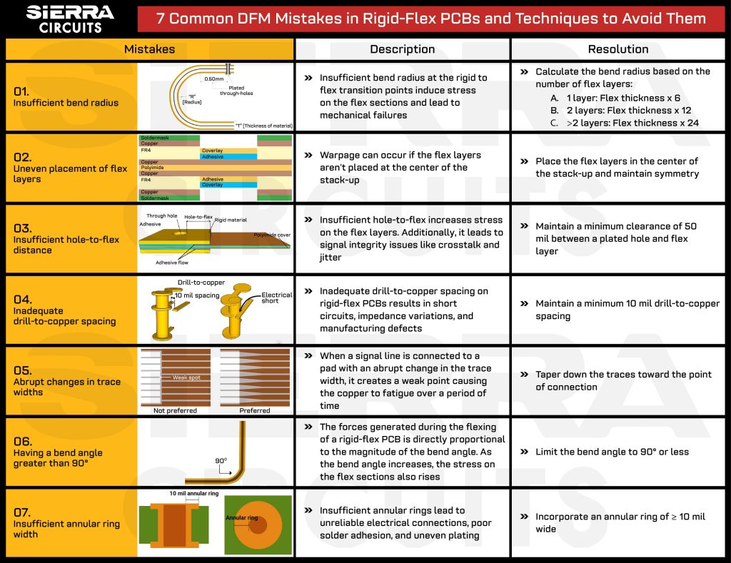
4. Not calculating the bend radius

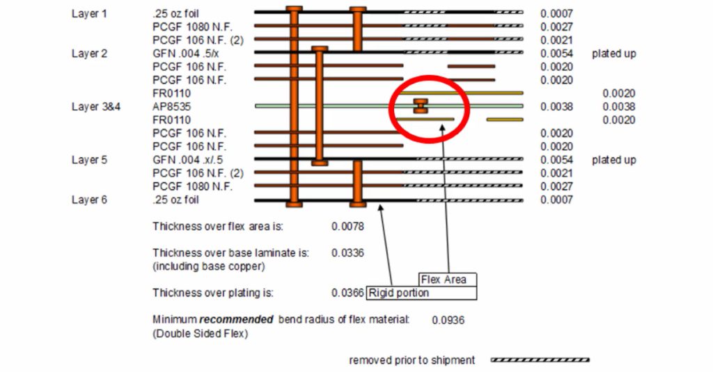
Lack of a sufficient bend radius for the flex portions can lead to the accumulation of stress, material fatigue, and eventual failure over time. When designing the flex region of a rigid-flex PCB, you must take into account the minimum bend radius. The minimum bend radius specifies how tightly the flex part may bend without harming the circuitry.
IPC-2223B standard provides the standards to compute the bend radius of a rigid-flex circuit board. It is determined by the number of layers your design has. You can determine the bend radius by referring to the table below.
| Number of layers | Bend radius (mils/mm) |
|---|---|
| 1 (single-sided) | Flex thickness x 6 |
| 2 (double-sided) | Flex thickness x 12 |
| Multi-layer | Flex thickness x 24 |
5. Having a bend angle greater than 90°
The forces created during circuit flexing, specifically tension on the outer side and compression on the inner side, rise proportionally with the bend angle. Thus, it’s best to bend a circuit as much as necessary to achieve the design goals.
Avoid bending a circuit at angles greater than 90°. For dynamic applications, where the circuit will undergo repeated flexing, flattening, and re-flexing, it is crucial to ensure that the bend angle does not exceed 90°.

6. Overlapping traces in a flex section
Stacked traces can decrease circuit flexibility and induce stress, leading to copper trace thinning at the bend radius. When engaging in double-sided flex routing, stagger the traces rather than having them overlap each other. By implementing this technique, we can effectively distribute the stress and minimize any potential damage. This can greatly enhance the overall durability and longevity of the conductors, ensuring optimal performance in various bending scenarios.


7. Insufficient hole to flex distance
Inadequate hole-to-flex spacing in a rigid-flex PCB leads to mechanical stress concentration, tearing of traces, signal integrity concerns, solder joint reliability issues, and electrical shorts. Hole-to-flex is the distance from the via to the flex-to-rigid transition area. To ensure high reliability, this clearance must be greater than 50 mil.

8. Using hole size less than 6 mil
The cost to manufacture a rigid-flex PCB increases as the hole size decreases, as it is more difficult to plate holes through adhesive-based materials. Always maintain a minimum hole size of 6 mil in the rigid area and 7.9 mils in the flex area. However, if the hole size is 15 mils and above, it doesn’t incur any additional cost.
Let’s look at the chart that depicts the relationship between cost and hole size.

To learn more about flex PCB cost drivers, see what are the cost drivers of flex PCBs
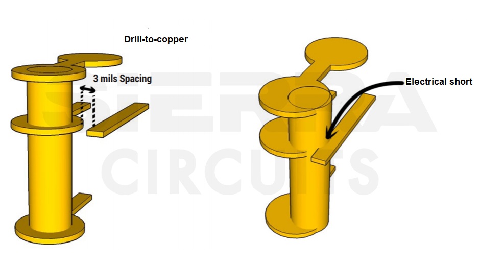
9. Inadequate drill-to-copper spacing
Insufficient spacing between drills and copper on rigid-flex PCBs can lead to various problems such as short circuits, fluctuations in impedance, weaknesses in mechanical integrity, difficulties in manufacturing, and challenges in soldering.
The standard drill-to-copper distance for flex is 10 mil, and anything under 7 mil will increase the manufacturing cost of the rigid-flex PCB exponentially.
10. Using a solid layer of ground plane
If the ground plane is poured as a solid area of copper, there is a potential risk of subjecting it to significant stress and thereby diminishing its flexibility.
Utilize a cross-hatched ground plane on the flexible area.

11. Unoptimized transition zones
In rigid-flex PCBs, the region where the flexible section of a circuit intersects with the rigid section is called the transition zone. This section is prone to exhibit defects such as adhesive squeeze-out, protruding of dielectric materials, crazing, and haloing. It typically consists of materials with rough edges. If the flex circuit is bent sharply against these rough edges, it can cause damage to the conductor paths.
For an efficient transition zone:
- Extend the flex coverlay into the rigid region to seamlessly integrate it with the rigid layers. This ensures a smooth and uninterrupted transition between the flexible and rigid sections.
- Ask your CM to apply flexible epoxy strain relief, and a bead of epoxy material at the transition area to ensure bend reliability and prevent inadvertent damage.

12. Changing trace width abruptly
When traces intersect pads, a sudden alteration in trace dimension gives rise to a vulnerable point. To avoid this, employ a teardrop configuration when altering the width of traces that link to pads and vias within flex circuits.

13. Ignoring the use of stiffeners
It may be necessary to provide supplementary reinforcement to regions such as the connector interface and the flex sections with components to increase the rigidity. Neglecting the incorporation of PCB stiffeners may result in the occurrence of stress concentrations. This leads to the board’s failure.
Here are a few guidelines to follow when you’re incorporating stiffeners in your design:
- Have an additional tolerance of 10-20 mils for the mechanical support holes when incorporating stiffeners. This precaution is necessary due to the potential for misalignment during manual assembly in subsequent stages.
- When utilizing multiple stiffeners, maintain the same thickness for all stiffeners.
- Avoid positioning stiffeners too close to vias or pins to prevent shorts.

Also read our case study: rigid-flex PCB design for an innovative helmet-mounted display to see how rigid-flex PCBs powered a compact, high-performance wearable solution.
Designing a rigid-flex board using Altium Designer
While designing a rigid-flex PCB, it’s important to ensure that the flex section will fold correctly and fit into an existing enclosure. Most design teams use a “paper doll,” which is a 1:1 printout of the PCB outline on paper. However, these paper dolls come with limitations, such as:
- Time-consuming and difficult
- Can’t accurately replicate flex bending
- Can’t accurately replicate rigid sections and stiffeners
- Difficult to attach components to paper to test other areas for fit
To overcome these limitations, you can use Altium Designer’s 3D rendering and simulation that helps you understand if the rigid-flex PCB will flex as intended and fit in an enclosure.
What should you include in your rigid-flex fab notes
Rigid section fab notes
- Board outline with dimensions
- Stack-up with all the thicknesses and impedance requirements
- Drill chart and drill legend for quality checks
- Board component data or any specific instructions to the CM
Flex section fab notes
- Dimensions and locations of stiffeners
- Locations of transition vias
- Drill map and drill legend for quality checks. Locations where the board will flex
- Thickness of all the flex sections and materials to be used
Creating a rigid-flex PCB using Altium Designer
While designing a hybrid PCB, it is crucial to keep in mind the above-mentioned DFM mistakes in rigid-flex PCBs to avoid unnecessary potential manufacturing errors.
In the next section of the webinar, John demonstrates an actual example of a rigid-flex PCB design that he designed using Altium Designer and fabricated with Sierra circuits. It is an MCU-based design that works with sensors.
In the webinar, John defines the steps to design a rigid-flex PCB:
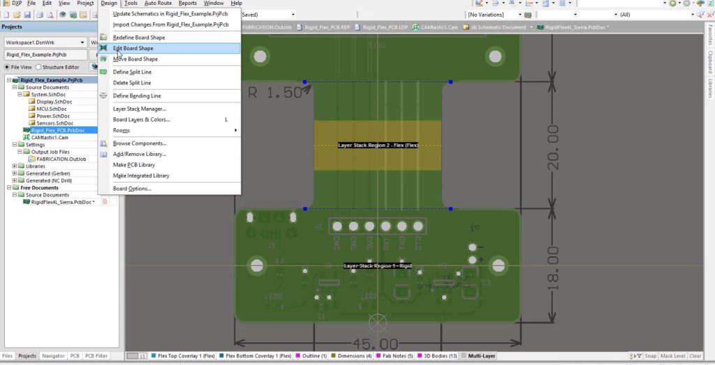
Step 1: Define rigid and flex layers
The first step in the creation of rigid-flex design is to work with a layer stack manager, where you define the specifics of each layer for both rigid and flex layers.

Step 2: Mark the boundaries of the outline and individual rigid/flex regions
The next step involves marking the boundary of the overall outline and using split lines to form different regions for both the flexible and rigid sections in the board planning mode. Here, you also define and name your rigid and flex sections.

Step 3: Set the design rules (DRC)
After the regions and bending are defined, the next step involves looking into design rules. Where designed rules are defined, both rigid and flex sections are defined as per Sierra rigid-flex design guidelines.

To learn the difference between DRC and DFM, see design rule check vs. design for manufacturing.
Step 4: Visualize flex movements
You can see the 3D view of your design in 3D rendering. Here, the flex sections can be stimulated based on the bending angles to verify if they fit perfectly within the mechanical enclosure.

Step 5: Generating fabrication output
Finally, once the design is complete, the next step is to generate the output in the output job line, where all the outputs are listed. Here, you can configure each output as per your requirements and generate Gerber files.

Key takeaways:
-
- DFM mistakes in rigid-Flex PCBs can lead to production delays, increased cost, and low product quality.
- Use low/no flow prepreg and adhesive/less adhesive for flex sections.
- Use symmetrical and even material layup. Place flexible layers in the center, and place vias at least 20 mil from the rigid-flex/flex interface.
- Avoid sharp turns; use curves instead of 45°/90° corners.
- Follow IPC-2223B standards; avoid bend angles greater than 90° for dynamic applications.
- Stagger traces for optimal flexibility.
- Maintain a minimum of 50 mil hole to flex clearance and 10 mil of drill-to-copper
- Use cross-hatched ground planes to improve flexibility.
- Ensure smooth integration between flex and rigid sections
- Use teardrop configuration to avoid abrupt trace width transitions.
- Incorporate stiffeners for structural reinforcement.
Rigid-flex PCB design is a complex process that necessitates technical knowledge, meticulous planning, and an observant eye for potential DFM mistakes. Avoiding common DFM mistakes in rigid-flex PCB such as improper material selection and routing, unoptimized stack-up, using excessive bend angles, neglecting bend radius, pad supports, stiffeners, insufficient clearances, and overlapping traces.
To ensure a reliable rigid-flex PCB, employ low or no prepreg, maintain symmetry in your stack-up, calculate the optimal bend radius, avoid sharp angles, stagger traces, and maintain adequate clearances between the copper features.
Please let us know in the comment section if you require any assistance in designing an error-free rigid-flex PCB. Our design experts will be happy to help.
Join SierraConnect today to gain access to a vast pool of circuit board design knowledge. You can use this forum to ask your PCB questions.
About Mohamed Faheemuddin : Mohamed Faheemuddin is a mechanical engineer. His passion for electronics drew him to the PCB industry. With an experience of over 3 years in the PCB industry, he specializes in developing articles for engineers and hardware designers.


Start the discussion at sierraconnect.protoexpress.com