


Contents

On-demand webinar
How Good is My Shield? An Introduction to Transfer Impedance and Shielding Effectiveness
by Karen Burnham
Air gap construction method in rigid-flex PCB manufacturing was introduced by the IPC to overcome the mechanical and electrical reliability issues in higher layer count rigid-flex designs.
In this article, we’ll go through various electrical and mechanical reliability issues and techniques to eliminate them in rigid-flex boards.
Consequences of having a higher layer count in rigid-flex PCBs
Laminating multiple layers into a single structure is a common way of addressing higher layer counts in a board design. This holds good for rigid circuit boards but it results in electrical and mechanical reliability issues in rigid-flex PCBs.
Mechanical reliability issues
The mechanical reliability of a flex board is determined by its bend capability. The bending capability of a flex circuit decreases as the thickness of the flex section increases. This is due to the increased strain placed on the copper circuitry. In a static application, a standard minimum bend radius for a 1 or 2-layer flex board is 10 times the flex thickness. For a 4-layered board, the bend radius value increases to 30 times the flex thickness. The circuit may break if it exceeds the minimum bend capability. A PCB manufacturer cannot change the physical properties of the utilized materials. However, the mechanical reliability issues such as increased strain in copper traces and bend capabilities are handled by changing the method of the construction.
Electrical reliability issues
Electrical reliability concern arises as a result of using inappropriate board materials. In a rigid-flex PCB, FR4 materials are used in the rigid sections and the layers in the flex section are laminated using epoxy or acrylic-based adhesives. The flex layers and the adhesives have a higher coefficient of thermal expansion (CTE) than FR4 materials. When a rigid-flex board is exposed to a high-temperature environment, the adhesives expand and shrink. Due to this, the via plating can be damaged resulting in open circuits.
What is air gap construction method in rigid-flex boards?
To address the reliability issues of rigid-flex PCB, IPC has developed a construction method known as air gap construction.
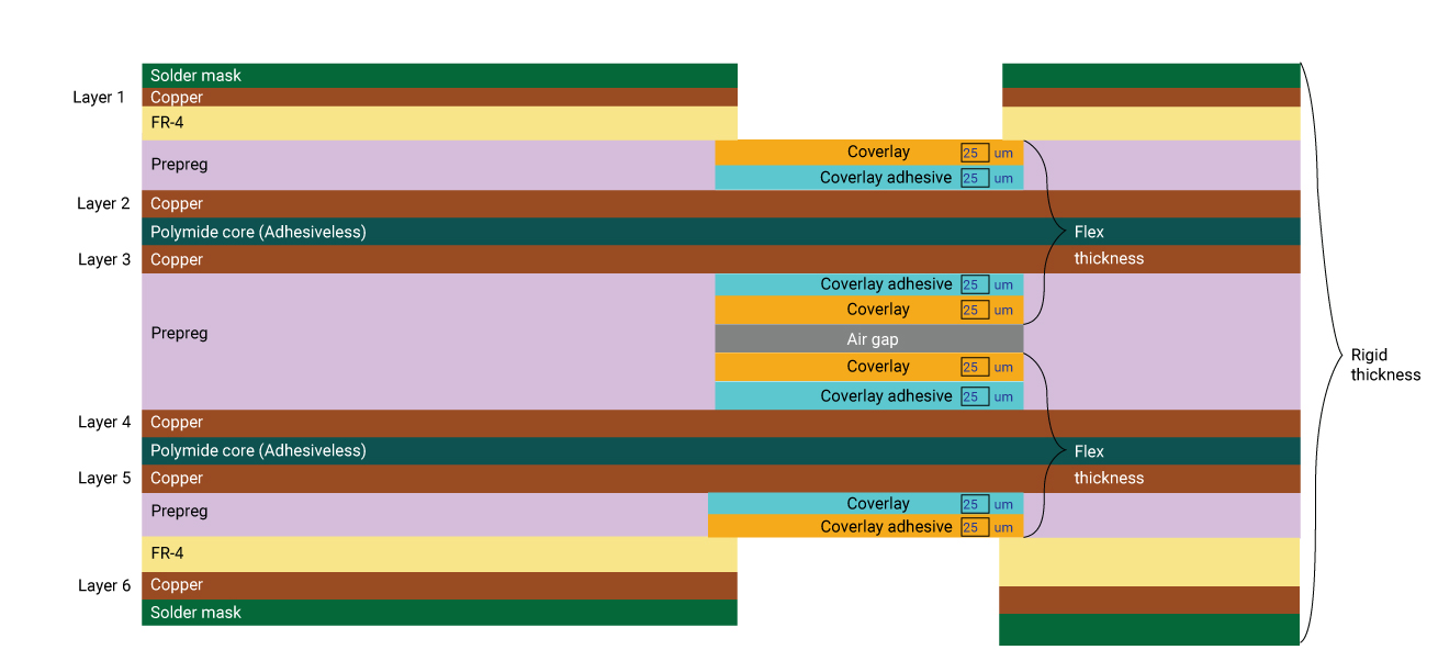
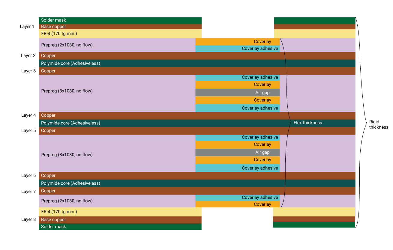
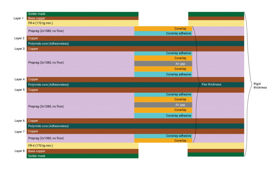
In air gap construction, the flex layers are kept as several independent sets of no more than three layers per set. Although 2 layers per set are optimum, the IPC 2223 standard allows for 3 layers, if a design incorporates controlled impedance lines in the flex area. Here, one layer can be configured as a stripline, with two adjacent layers acting as shields. As seen in the above PCB stack-ups, the air gap construction eliminates the flex adhesives within the rigid sections. This also addresses the via hole reliability issues.

How does air gap construction address via reliability issues?
Earlier, rigid-flex boards were fabricated by implementing many layers of adhesives within the rigid section. The coefficient of thermal expansion (CTE) of these adhesive layers is very high when compared to standard FR-4 materials. As a result, vias undergo a significant amount of stress during the assembly process and while operating in a high-temperature environment. An air gap in rigid-flex PCB solves the via reliability problem, as it completely eliminates the use of adhesive in the rigid section.
In this method, the flex layers are separated by prepregs present in the rigid area. This not only solves the via reliability problem but also improves the adhesion between the rigid sections.
Although an air gap rigid-flex PCB requires more process steps, the enhanced reliability of this type of structure saves costs in the longer run. To learn more about how rigid-flex boards reduce the overall cost of electronic devices, see rigid-flex cuts electronic product assembly costs.
How air gap construction improves mechanical flexibility and bend capability
An air gap architecture considerably improves the bending capability of flex boards. The following two factors are responsible for these improvements:
- The flex thickness of each individual flex layer is significantly reduced when compared to a totally laminated construction. This not only improves the flexibility but also reduces the I-Beam effect.
- Each flex layer is permitted to bend independently based on its thickness, with little interference from the other flex layers.
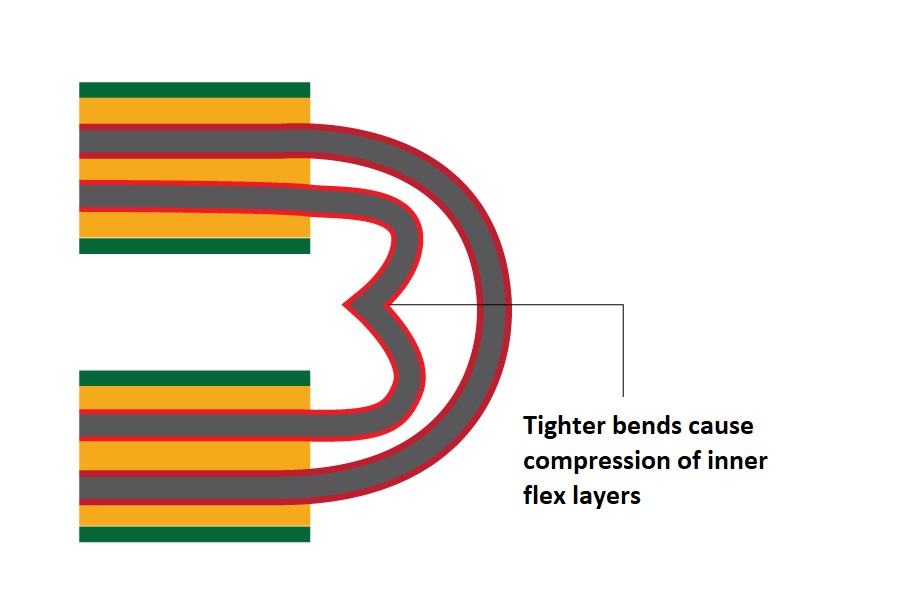
Individual flex layers are allowed to bend to their natural radius. As the air gap space between layers is exhausted, they may get into contact with each other. In an extreme U-shaped bend requirement as shown in the image above, the outer flex layer may confine the inner flex layer till it buckles. Any buckling of a flex layer beyond the material’s capabilities would result in fractured circuits, hence this circumstance must be avoided.
To explore how air gap construction enhances mechanical flexibility and bend capability, read our case study implementing a loose-leaf rigid-flex PCB stack-up for enhanced flexibility.
PCB interconnect stress testing
Interconnect stress testing (IST) is a technique to detect failures in vias and PTHs of an air gap in rigid-flex PCB construction. This test is carried out on a test coupon, which is subjected to a series of thermal cycles. Here, the via barrels and the PTHs are continuously exposed to current until the board passes the reliability test. The temperature ranges from 25 to 150°C.
The advantages of IST are listed below:
- Environment-friendly and cost-effective
- Detects failure during the early phases of fabrication
- It can be used to estimate the life of a PCB
- Provides a simplified analysis of the circuit board within a quick time
Also read, 13 common DFM mistakes in rigid-flex PCBs and techniques to avoid them.
6 standards of IPC 2223 that impact the reliability of flex PCB
IPC 2223 standard provides detailed information that covers all the crucial elements of rigid-flex designs. In this section, we will have a look at 6 major standards that impact the reliability of flex boards.
Via keep out areas in the flex transition zone
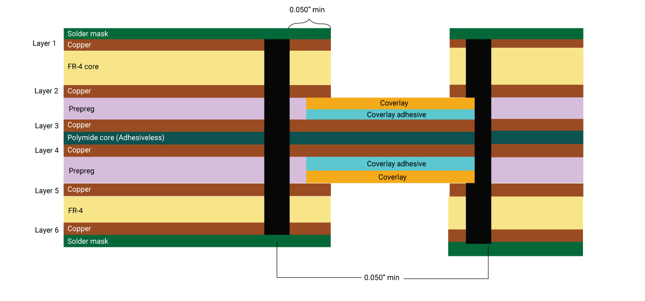
The location of any plated vias or holes in relation to the flex transition zone is a crucial factor that affects the reliability of rigid-flex boards. The coverlays must protrude with the rigid sections by a minimal distance to ensure that they are laminated within the rigid area. The coverlays are laminated to the flex section using an adhesive (acrylic or epoxy). The coefficient of thermal expansion of these adhesives is extremely high. Vias drilled through an adhesive layer are vulnerable to stresses generated by the adhesive’s thermal expansion and contraction. When these vias are exposed to high temperatures, the via plating can be damaged, posing a serious issue.
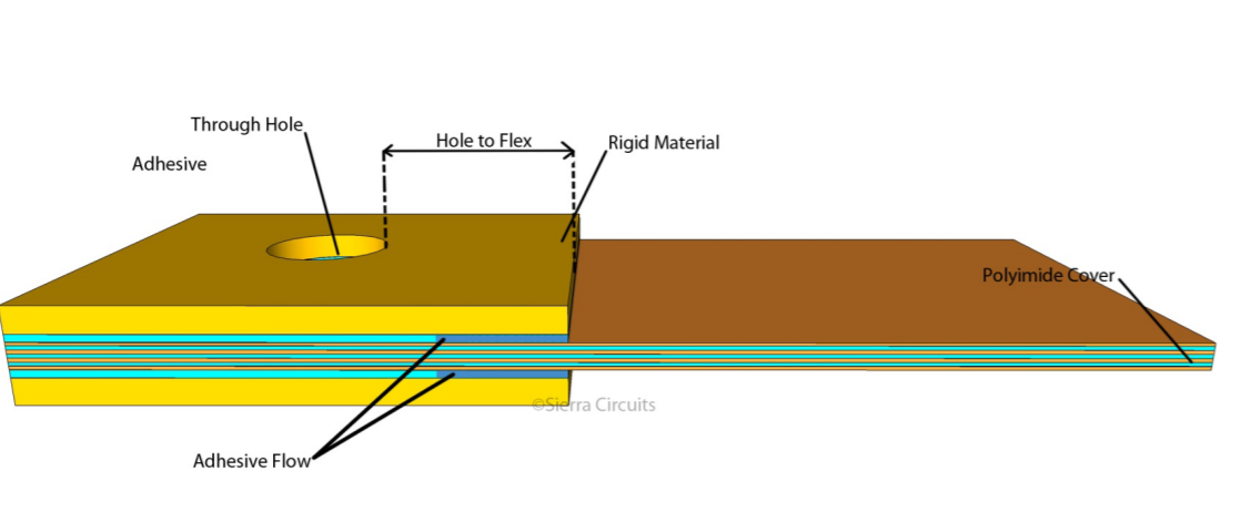
IPC 2223 recommends a minimum distance of 0.125” between vias and the rigid-flex transition area. However, it is possible to avoid vias through the coverlay with a shorter spacing. We recommend at least a 50 mil (0.05″) distance between the hole and the flex section. Sometimes, this hole to flex distance is 30 mil for commercial applications.
Rigid-flex selective coverlay construction
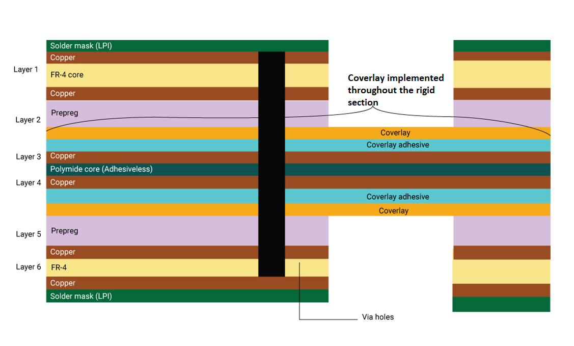
The manufacturing process of flex boards has evolved due to increased design complexity, the requirement of smaller via holes, and increased assembly temperatures. Earlier, coverlays were implemented throughout the rigid section. As a result, vias and PTHs were drilled through the adhesives layers which causes via reliability concerns.
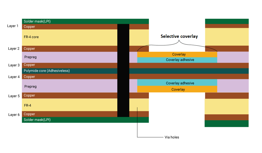
IPC 2223 recommends having the coverlays selectively on the flex sections, with a minimal distance of engagement into the rigid region of the board. This approach also has the advantage of not having coverlays or adhesives in the rigid area, resulting in a stronger lamination. It is important to specify that the board should be fabricated using the selective coverlay construction method in the fabrication drawing.

Adhesiveless flex cores
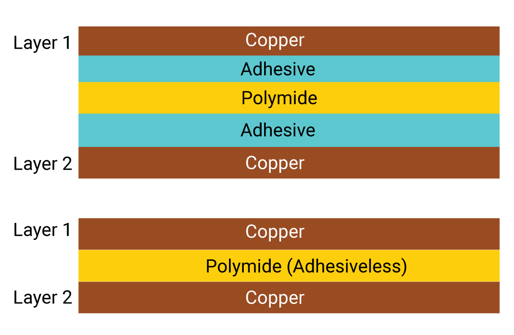
The flex core materials must adhere to IPC 2223 criteria.
Flex PCB materials exist in two categories:
- Adhesive based: copper layer is bonded to the polyimide with acrylic adhesive.
- Adhesiveless: copper is cast directly onto the polyimide.
IPC 2223 promotes the use of adhesiveless flex cores only. Employing adhesiveless flex cores eliminates a source of adhesive from the rigid regions. This also eliminates the reliability issues discussed in the earlier sections. An additional advantage of using adhesiveless flex materials is that it has a reduced thickness when compared with adhesive based materials. Thinner flex cores increase the flexibility and bend capability of the flex PCB.

PCB Material Design Guide
9 Chapters - 30 Pages - 40 Minute ReadWhat's Inside:
- Basic properties of the dielectric material to be considered
- Signal loss in PCB substrates
- Copper foil selection
- Key considerations for choosing PCB materials
Download Now
Minimum bend radius capabilities
Assuring the flex board meets the bend criteria is important for a successful design. A flex section’s bend capability is determined by the materials and the thicknesses utilized. Minimum bend recommendations are provided by IPC 2223 standards for both static and dynamic applications. The minimum bend radius is determined by the flex thickness multiplied by a factor that depends on the layer count. The tables below define the bend requirements for static and dynamic applications.
Bend requirements for static applications
| Number of layers | Minimum bend radius |
|---|---|
| 1 to 2 | 6 times the flex thickness |
| 3 or more layers | 12 times the flex thickness or more |
Bend requirements for dynamic applications
| Number of layers | Minimum bend radius |
|---|---|
| Limited to 1 or 2 layers | 100 times the flex thickness |
IPC 2223 also allows a flex section to be bent and creased with a zero bend radius if certain standards are followed. This is limited to very thin one and two-layer constructions, with the additional restriction that the flex cannot be unfolded once it has been creased. In the fold area, a PSA (pressure-sensitive adhesive), is frequently used to firmly affix the flex and prevent it from being accidentally unfolded.
Strain relief fillets
A strain relief fillet is a flexible bead made of epoxy. These fillets are generally applied to the rigid-flex transition zones. Fillets enable the flex to bend gradually rather than being bent tightly. Implementation of fillets reduces the chances of damage in the copper circuitry around the transition zone.
IPC 2223 specifies a minimum 0.010” vertical spacing between the rigid section and the flex layers. This ensures optimum spacing for the bead to prevent it from reaching the adjacent rigid section. The fabrication drawing specifies the strain relief needs.
Pre-bake requirements
According to IPC 2223, pre-baking flex circuits prior to assembly is an industry-standard requirement. This rule applies to all flex and rigid-flex designs made of polyimide.
Delamination of the coverlays and/or rigid sections will occur if moisture is not removed. Additional pre-bakes may be necessary if many assembly cycles are required. Pre-baking takes place at 120°C for 2-10 hours, depending on the design. Airflow across all sides of the board can be set in the pre-bake oven.
The air gap construction method enables PCB designers to achieve tighter bend requirements and eliminates the reliability issues related to via plating, mechanical bending, and electrical stability. Let us know in the comments section if you are facing any design-related challenges. We will be happy to help you out.
Flex PCB Design Guide
10 Chapters - 39 Pages - 45 Minute ReadWhat's Inside:
- Calculating the bend radius
- Annular ring and via specifications
- Build your flex stack-up
- Controlled impedance for flex
- The fab and drawing requirements
Download Now
About Milan Yogendrappa : Milan Y is an electronics and communication engineer with over 6 years of experience in developing and editing technical articles related to PCB design, manufacturing, and assembly. He is currently the editor-in-chief at Sierra Circuits.


