



Contents

On-demand webinar
How Good is My Shield? An Introduction to Transfer Impedance and Shielding Effectiveness
by Karen Burnham
Ultra-HDI PCBs are becoming essential in high-speed applications such as AI systems, where circuit density and signal integrity are critical. As operating frequencies go beyond 25 GHz, even small variations in line width, spacing, and impedance can lead to significant signal losses.
UHDI technology supports extremely fine features and tight tolerances, making it possible to maintain signal quality while accommodating the dense routing and component demands of advanced systems.
Highlights:
- Ultra-HDI PCBs use ultra-fine features, with trace and space dimensions of 2 mil or less.
- They rely on advanced structures like laser-drilled microvias, via-in-pad connections, and thin dielectrics instead of traditional plated through-holes.
- Modern fabrication methods, such as SAP/mSAP and embedded trace technology, help overcome the challenges in fabricating UHDI boards.
In this article, you’ll learn UHDI PCB defining features, key design considerations, fabrication challenges faced by manufacturers, and emerging trends.
Before we dive into the technical part, here’s a brief overview of the UHDI PCB market size.
Global and North American ultra-HDI PCBA market projections (2022–2030)
The Ultra-HDI PCB market is experiencing rapid growth, driven by an industry-wide shift toward miniaturization. Fab houses are increasingly adopting UHDI manufacturing techniques to meet this requirement.
The global Ultra-HDI circuit board market is projected to grow from US $1.68 billion in 2025 to US $3.07 billion by 2030, reflecting a CAGR of 10.2%.

The U.S. CHIPS Act of 2022 is set to further boost domestic capabilities in North America, particularly in areas such as advanced packaging and chiplet-based substrate technologies. The North American market is projected to expand from US $0.79 billion in 2025 to US $1.52 billion by 2030, at a CAGR of 11.1%.

Source: Sierra Circuits’ market research analysis report derived from the annual reports of PCBA industry leaders.
What are ultra-HDI PCBs?
UHDI printed boards are advanced circuits designed to achieve extremely high routing density. They use trace widths and spacings finer (<2 mil) than those in conventional HDI technology. These boards are widely used in IC packaging. They have ultra-fine lines, microvias, via-in-pad, and very thin build-up layers to fan out thousands of I/O connections from the chip.

| Parameter | Features |
|---|---|
| Conductor width and spacing | ≤50 µm (2 mil) |
| Dielectric thickness | <50 µm (2 mil), significantly reducing overall board height |
| Microvia diameter | <75 µm (3 mil), freeing space for dense trace routing across the board |
| Stack-up | Increased routing density can reduce layer count |
To learn how to design reliable HDI PCBs, download our eBook.
HDI PCB Design Guide
5 Chapters - 52 Pages - 60 Minute ReadWhat's Inside:
- Planning your stack-up and microvia structure
- Choosing the right materials
- Signal integrity and controlled impedance in HDI
- Manufacturing considerations for higher yields
Download Now
Standard vs. HDI vs. UHDI printed boards
The infographic below summarizes the differences among standard, HDI, and UHDI PCB technologies.
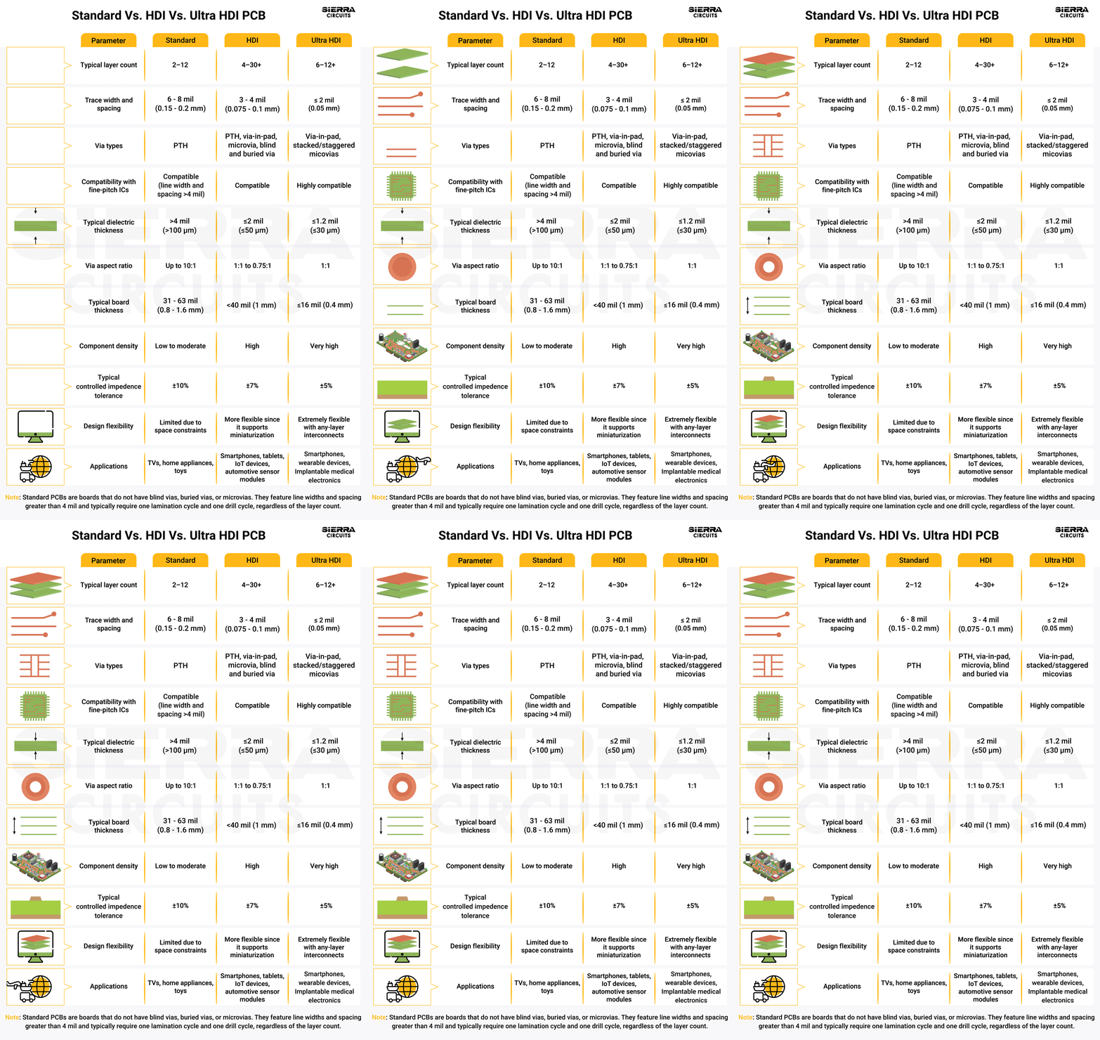
Steve Carney, R&D Project Manager, explained that the main difference between HDI and UHDI is the much lower trace width achievable in UHDI designs. The manufacturing complexity increases as the trace width value decreases.
Dielectric material requirements for UHDI circuit boards
In UHDI boards, material plays a critical role in achieving finer features and long-term reliability.
Standard PCB materials, even advanced flat/spread glass laminates, are not suitable for laser drilling. They also cannot withstand the repeated press cycles required for sequential lamination.
To support ultra-HDI structures, fabricators implement specialized build-up films such as Ajinomoto (ABF), BT resin, modified epoxy, polyimide, and LCP. Very low-profile (VLP) copper foils are also used with these dielectrics to enable ultra-fine line/space features and stable signal performance. These materials use either a non-reinforced or a modified reinforcement system with much finer glass than standard cloth.
Build-up films are laminated to the rigid core layer of standard PCB materials to enable the formation of multiple layers with finer traces and vias. These films are designed specifically for micro-laser drilling. They can endure numerous lamination cycles while delivering excellent electrical properties.


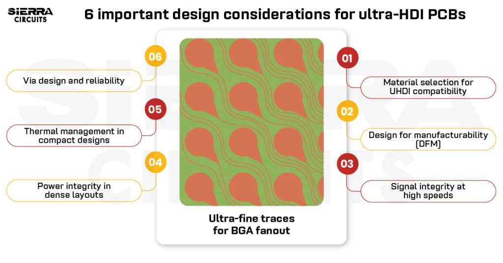
6 important design considerations for ultra-HDI boards
Before designing your layout, you need to consider system-level constraints that impact signal integrity, power delivery, thermal performance, and material behavior. Addressing these factors early helps prevent design errors and aligns the layout with your fabricator’s capabilities:
IPC is still working on the specs for UHDI technology. For baseline high-density design standards, refer to IPC-2226.
1. Material selection for UHDI compatibility
-
- Choose advanced materials like build-up films (e.g., Ajinomoto ABF, BT resin, modified epoxy, or LCP) or high-Tg laminates to support laser drilling and withstand sequential lamination cycles.
- Select materials with low dielectric constants (Dk 2.8–3.5) to enhance signal integrity and thermal stability.
2. Design for manufacturability (DFM)
-
- Engage with your PCB fabricator from the earliest stages of design to confirm their capabilities for minimum trace/space, via sizes, layer stack-ups, and material compatibility.
- Understand the strengths and limitations of different UHDI manufacturing methods, such as subtractive, mSAP, SAP, or embedded, and customize your design accordingly.
-
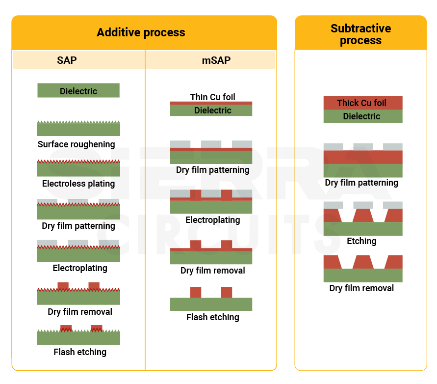
Comparison between additive and subtractive PCB manufacturing processes. To learn about the common DFM and DFA mistakes, see the top DFM and DFA mistakes that delay your PCB production.
3. Signal integrity at high speeds
-
- Ensure consistent impedance for the traces carrying signals above 25 Gbps to minimize reflection and attenuation.
- Apply high-speed layout techniques, such as differential pair tuning and length matching. For high-speed routing techniques, see the 11 best high-speed PCB routing practices
- Route critical signals on inner layers and minimize via usage to reduce crosstalk and signal degradation.
4. Power integrity in dense layouts
-
- Design tightly packed power distribution networks to limit IR drop and noise.
- Strategically place decoupling capacitors in dense grids and utilize embedded components to stabilize power delivery.
5. Thermal management in compact designs
-
- Manage localized hot spots caused by thin dielectrics and dense component placement, which can degrade performance.
- Implement thermal vias, copper planes, heat spreaders, and, in advanced cases, microfluidic or integrated cooling methods. For heat dissipation techniques, see 12 PCB thermal management techniques to reduce heating.
6. Via design and reliability
-
- Ensure your microvia design adheres to the fabricator’s aspect ratio limits and uses high-quality fill materials to maintain reliability under thermal and mechanical stress.
- Use via-in-pad configurations to maximize routing density while maintaining structural integrity.
- Avoid PTHs that start or end on UHDI layers to reduce complexity and prevent potential manufacturing problems.
To learn how to build reliable vias in your high-speed boards, see 4 RF PCB via design challenges with layout solutions.
In addition to the above, perform thermal simulations and signal integrity analysis to ensure the design meets the performance standards. Always get your fabricator’s approval for your stack-up, and aim for a symmetrical design. Designs with an odd number of layers require extra care during fabrication to avoid potential issues.
Check Sierra Circuits’ HDI PCB capabilities to learn more.
6 challenges in fabricating UHDI PCBs
1. Tight tolerance control
As trace widths shrink, tolerance demands become extreme. For instance, etching 3-mil traces can be done with ±10% tolerance (~0.0003”). However, when the trace width decreases to 2 mil, the tolerance increases to ±15%, and at 1 mil, it rises to ±30%, making production extremely difficult. Achieving a tolerance of ±0.1 mil presents a significant technical challenge.
Fabricators address this with advanced laser direct imaging (LDI), fine-line etching chemistry, and mSAP processes that improve dimensional accuracy.
2. Etch profile degradation
Traditional subtractive processes yield trapezoidal traces with inconsistent sidewalls. This geometry is not suitable for UHDI applications where clean, rectangular profiles are needed.
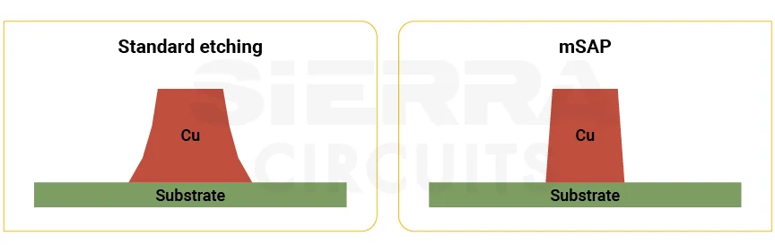
When subtractive methods reach physical limits below 2-mil features. Fab houses implement SAP and mSAP processes to ensure rectangular traces with tolerances as tight as ±0.1 mil.
3. Handling damage
Ultra-fine traces are physically fragile and more prone to damage during lamination and panelization. Fabricators use automated handling systems, protective carrier panels, and controlled lamination pressure to minimize defects.
4. Cleanroom and environmental controls
UHDI fabrication demands advanced process control, including cleanroom environments and stringent humidity/temperature regulation, to ensure material stability and dimensional accuracy. Manufacturers employ cleanrooms with real-time environmental monitoring to avoid any contamination.
5. Equipment limitations
Standard PCB lines are often incapable of UHDI production. It requires high-resolution laser imaging, advanced direct plating, and microvia drilling with sub-50 µm accuracy. Fab houses use UHDI-ready equipment such as UV/CO₂ lasers, precision plating systems, embedded trace processes, and X-ray registration tools to enable consistent production of ultra-fine features.
6. Material compatibility
Typical dielectric materials can degrade under repeated lamination cycles or fail to support laser-drilled vias, requiring specialized resin systems or buildup films. As a PCB designer, you need to pick advanced buildup films, low-loss resins, and high-Tg dielectrics designed for UHDI processes to overcome material degradation issues and support fine-pitch interconnect structures.
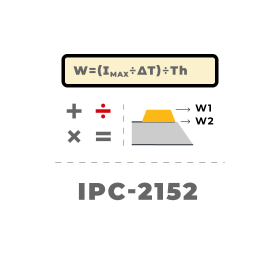
Try our tool to determine the best trace width for your designs.
Key technologies that enable the production of UHDI printed circuit boards
SAP and mSAP manufacturing techniques
SAP (semi-additive process): A PCB fabrication method that forms circuit patterns by adding copper to the dielectric instead of etching it away.
mSAP (modified semi-additive process): An improved version of SAP that enables finer line widths and spacing.
Since circuit board etching is a critical step, both SAP and mSAP employ extremely thin base copper or conductive layers to minimize the exposure time of traces to the etchant. Reducing etching time helps prevent sidewall damage to the traces.
Any imperfections in the trace geometry, such as width reduction, undercutting, or notching/mouse bites, can degrade signal speed and compromise signal integrity.
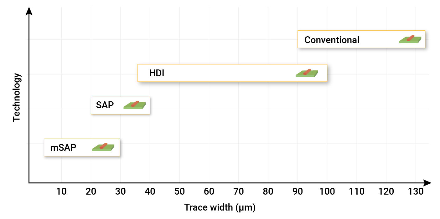
The relationship between achievable trace width and process technology is critical for UHDI success. The figure demonstrates the superior trace width capabilities of SAP/mSAP compared to conventional processes across UHDI requirements.
Embedded trace technology
This technology is based on trenching cured dielectric material to form the traces. Sierra Circuits holds multiple patents covering embedded trace technology.
The process involves:
- Pattern creation: Cutting trace patterns into dielectric using laser/plasma process.
- Metallization: Electroplating copper into trenches
- Planarization: Flattening the surface
This technology has three major advantages:
| Advantages of embedded trace technology | Technical impact |
|---|---|
| 1. Trace stability during lamination | Since the trace pattern is cut into the cured dielectric, it remains stable and does not shift during lamination. In contrast, SAP and mSAP processes often experience trace movement due to heat and pressure, especially affecting capture pads for laser vias. |
| 2. Protection from etchant | Traces embedded below the surface are shielded from the etching process, preventing sidewall damage and ensuring a consistent trace profile. |
| 3. Additive plating and improved signal speed | Trench plating is a fully additive process, requiring no base foil or adhesion promoter. This eliminates the need for roughened surfaces (like dendrites), leading to improved signal speed. |
Download our eBook for design for manufacturing guidelines.
Design for Manufacturing Handbook
11 Chapters - 96 Pages - 90 Minute ReadWhat's Inside:
- Annular rings: avoid drill breakouts
- Vias: optimize your design
- Trace width and space: follow the best practices
- Solder mask and silkscreen: get the must-knows
Download Now
8 design benefits of ultra-HDI technology
- Maximizes component density: Enables placement of more components and interfaces on a single PCB through ultra-fine features (traces/vias), fitting advanced functionality into smaller devices.
- Reduces system size and weight: Achieves significant miniaturization through lower layer counts, efficient microvia architectures (stacked and staggered vias), reduced drill cycles, and fewer lamination steps.
- Improves signal integrity: Shortens critical signal paths and minimizes parasitic capacitance/inductance by reducing loop areas and via stubs, leading to lower attenuation, reduced crosstalk, and cleaner signal transmission.
- Enables tighter impedance control: Achieves highly consistent ultra-fine trace widths/spacing (down to 15µm) and smooth copper profiles (via mSAP processes), allowing precise control of dielectric spacing and characteristic impedance (< 5% tolerance) essential for high-speed designs.
- Facilitates extreme routing density: Supports complex routing in minimal space through ultra-fine features and high aspect ratios 1:1 through advanced fabrication, enabling tighter packing without signal degradation.
- Improves biocompatibility for medical devices: Facilitates use of noble metals (e.g., gold) instead of copper/nickel for conductive traces, enhancing safety for medical implants, wearables, and micro-sensors.
- Enhances reliability with advanced structures: Improves mechanical robustness and frees up surface area using microvias created through sequential lamination and laser drilling, reducing failure points versus through-hole vias.
- Optimizes high-frequency/RF performance: Supports ultra-low-loss signal transmission at mmWave frequencies (5G, 6G, radar) and high-speed digital applications (DDR5/6, PCIe) through shorter paths, reduced component parasitics, tight impedance control, and compatible low-loss dielectrics.
Future trends in UHDI PCB development
As electronics have been largely adopting system-in-package (SiP) designs and chiplet-based architectures, UHDI PCBs can be foundational in delivering the extreme interconnect density these technologies demand.
At the same time, materials innovation is opening new frontiers. Glass substrates, high-Tg polyimide films, and advanced organic laminates are being adopted for their dimensional stability and processing advantages.
Additive processes like laser direct structuring (LDS) and inkjet printing are extending UHDI capabilities into 3D interconnects and rapid prototyping. In parallel, the integration of passive and active components like resistors, capacitors, and even silicon dies directly into the substrate is shaping the next generation of embedded system-in-substrate platforms.
Key takeaways:
- Collaborate early with your PCB fabricator to validate stack-ups, process capability, and manufacturability.
- Make sure your fabricator implements SAP/mSAP or embedded trace techniques to achieve trace accuracy, sidewall integrity, and high-speed performance.
- Select build-up films over standard glass-reinforced laminates to support laser drilling and multiple press cycles.
- Implement buried microvias and vias-in-pad to reduce layer count.
- Account for tighter etching tolerances, as they increase significantly as the trace widths reduce.
- Avoid PTHs through UHDI layers and validate signal integrity using simulation techniques like thermal and SI analysis.
- Stay informed on emerging UHDI IPC standards, as current HDI guidelines (IPC-2226) do not fully address <50μm trace/space designs.
Ultra-HDI PCBs require advanced fabrication processes like SAP, mSAP, and embedded trace technology. Know your fabricator’s capabilities before finalizing the design features to avoid board respins.
Have questions about ultra-HDI printed circuit boards? Post your queries on SierraConnect. Our PCB experts will answer them.

About Mohamed Faheemuddin : Mohamed Faheemuddin is a mechanical engineer. His passion for electronics drew him to the PCB industry. With an experience of over 3 years in the PCB industry, he specializes in developing articles for engineers and hardware designers.





Start the discussion at sierraconnect.protoexpress.com