Contents

On-demand webinar
How Good is My Shield? An Introduction to Transfer Impedance and Shielding Effectiveness
by Karen Burnham
Harry Kennedy, an electrical engineer and technical specialist at Altair, has shared his expertise in optimizing PCB designs for testing at PCB West 2023.
Highlights:
- Use 2-ounce or 1.5-ounce copper on the top layer to enhance heat dissipation.
- Perform simulations for a deeper understanding of pre-manufactured board performance.
- Design reviews should be collaborative, involving key stakeholders and experts like RF or signal integrity engineers.
Watch the full video to learn more:
What specific challenges do you encounter when testing PCBs, and how do you address them?
Harry Kennedy: When we’re working on PCB designs, the first step is ensuring that we have the correct components to actually perform the function. So, understanding the role of the main IC and identifying the need for supporting resistors, capacitors, or other devices is essential.
When we pick the right products and components, it’s crucial to check if they all work seamlessly together. Simultaneously, you should focus on minimizing heat and ensuring reliable signal integrity as you design the traces and incorporate the components into the layout.
Make sure you have the right components, as component selection is key to solving other potential issues. These issues could range from managing thermal concerns to accommodating higher-frequency requirements. It also plays a critical role in ensuring that we actually design boards that are manufacturable.
Design for Testing Handbook
7 Chapters - 28 Pages - 45 Minute ReadWhat's Inside:
- PCB testing strategies
- Guidelines to design and place a test point for FPT
- Directives to make your board ICT compatible
- Benefits and drawbacks of various testing methods
- Defects that you can identify through board testing
Download Now
How do you overcome solder fatigue concerns when selecting component packaging types?
Harry Kennedy: Solder fatigue is a significant concern, especially in industries like automotive, where safety is paramount. If you think about it, a malfunctioning circuit board in a vehicle can pose serious risks to people’s lives, so the stakes are high. Solder fatigue can occur due to thermal cycling and the constant vibrations experienced by a car. Understanding how these factors can impact your critical components is crucial.
The way I approach this process begins with a thorough understanding of the data sheets for the components I’m using. Manufacturers design these components with the real-world environment in mind. So, it’s important to ensure that we select the right packaging for the parts we use. Additionally, there are valuable tools and resources available, such as solder fatigue calculators.
These tools use mathematical models to predict the effects of temperature cycles and vibrations on the PCB. They also assess how these factors will affect the solder joints over time. This not only helps us identify potential points of failure but also allows us to assess how these failures might spread to the solder ball and the subsequent consequences.
What are the PCB testing methods a designer needs to specify to his manufacturer?
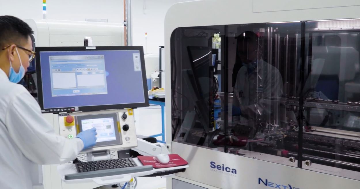
Harry Kennedy: The partnership with the manufacturer is always the key. Many engineers do not do checks. They simply send their designs to the manufacturer and await their feedback, but this approach is not very efficient.
Firstly, if there are challenges or modifications, you might have to uproot many of your components and rebuild a significant portion of your board. This requires both time and financial resources to implement those changes.
The second point to consider is that if the manufacturer attempts to build a board’s part repeatedly but fails, it results in wasted time and the generation of scrap materials. Ideally, the manufacturer should inform you when they can’t successfully build it. However, some engineers have experienced a situation where their faulty board design reaches the PCB assembly stage. It becomes evident that it won’t function correctly because the manufacturer didn’t create it accurately.
Therefore, it’s crucial to ensure optimum component spacing. This is essential for understanding potential issues that may arise with copper or solder resist. Ensuring the correct spacing is maintained for applying copper and solder resist onto the board is vital. Additionally, the spacing between traces is important. And the PCB etching process should be precise. Hence, if you don’t have a manufacturer who communicates their capabilities effectively, you may encounter problems with the yield.
The table below shows the recommended part-to-part spacings for different types of components.
| Chip | SOT | SOIC | PLCC | QFP | BGA | Axial | PTH | |
|---|---|---|---|---|---|---|---|---|
| Chip | 10-20 | 15-25 | 20-25 | 50-75 | 50-120 | 75-120 | 50-75 | 50-75 |
| SOT | 15-25 | 15-25 | 20-25 | 50-75 | 50-120 | 75-120 | 50-75 | 50-75 |
| SOIC | 20-25 | 20-25 | 30-50 | 50-100 | 75-120 | 75-120 | 50-75 | 100-150 |
| PLCC | 50-75 | 50-75 | 50-100 | 100-120 | 100-120 | 100-120 | 100-150 | 100-150 |
| QFP | 50-120 | 50-120 | 75-120 | 100-120 | 100-120 | 75-120 | 100-150 | 100-150 |
| BGA | 75-120 | 75-120 | 75-120 | 100-120 | 75-120 | 100-120 | 100-150 | 100-150 |
| Axial | 50-75 | 50-75 | 50-75 | 100-150 | 100-150 | 100-150 | 100-150 | 100-150 |
| PTH | 50-75 | 50-75 | 100-150 | 100-150 | 100-150 | 100-150 | 100-150 | 100-150 |
| **Dimensions given in this table are specified in mils | ||||||||
For detailed part placement and spacing guidelines, see component placement guidelines for PCB design and assembly.
The third aspect to consider is a thorough understanding of the spacing between components and the board edge. Especially when you’re striving to make devices more compact, it’s crucial to assess whether there is sufficient space between through-hole components or connectors and the board edge. This prevents long-term damage, like connectors breaking off, because the structural integrity of the board was not maintained during manufacturing.
What are the prevalent DFM checks?
Harry Kennedy: DFM checks primarily involve examining spacing. We assess component-to-component, component-to-trace, and trace-to-trace clearances.
Additionally, it’s important to note that these rules can vary based on the specific design. For instance, if your board has both a high-speed section and a high-power section, each of them may have distinct tolerances and spacing requirements. It’s crucial to ensure that these specific requirements are integrated into your DFM process.
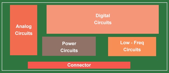
Another important consideration is the placement of components on one side of the board without anything underneath them. It’s crucial to perform checks for this scenario because there are certain components that shouldn’t have anything beneath them. These could be sensitive signal components or components with leads that need to pass through the board.
Design for Manufacturing Handbook
11 Chapters - 96 Pages - 90 Minute ReadWhat's Inside:
- Annular rings: avoid drill breakouts
- Vias: optimize your design
- Trace width and space: follow the best practices
- Solder mask and silkscreen: get the must-knows
Download Now
How do you manage thermal performance for your PCBs?
Harry Kennedy: Thermal performance is unquestionably a critical consideration. When dealing with power switching or power converters, managing thermal issues becomes crucial. To address this, you need to select components that excel at dissipating heat. This might involve thermal pads underneath the part. Alternatively, it may entail evaluating the size and area of those thermal pads in the decision-making process.
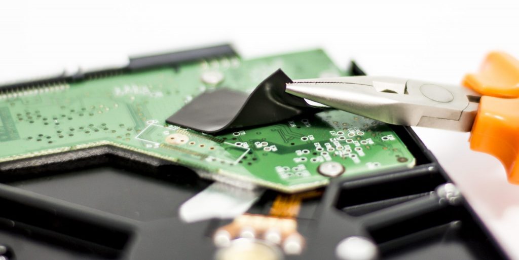
The second aspect to consider is the PCB design itself. For instance, if you have a thermal pad on one of your components, you may need to employ a technique to ensure that the copper on the top layer of your board efficiently dissipates heat evenly. This can be achieved using techniques such as the dog bone method, where you create copper pours on both the top and bottom of the thermal pad to create a pathway for heat dissipation.
Additionally, examining the layers within the stack is crucial. For instance, on the top layer, you might consider using 2-ounce or 1.5-ounce copper instead of the standard 1-ounce copper. This adjustment can enhance heat dissipation. However, you’ll have a trade-off with the cost. However, if it keeps your components running at cooler temperatures, it can ultimately add value to your final equipment.
Lastly, as designers, it’s essential to understand the system in which your board will be integrated. You can employ certain techniques, such as adding heat sinks to components that generate a significant amount of heat or incorporating a fan into the setup. For instance, if your system is enclosed in a box, you might consider the option of installing a fan to circulate air, which can effectively reduce overall system heat.
So, not only is it crucial to comprehend the thermal dynamics of your board, but also to be aware of your system’s requirements. If you can introduce solutions at a system level to address potential heat issues, it can be highly beneficial. Identifying these factors early in the design process is always key.
See what Keven Coates has to say about PCB heat dissipation techniques.
What does an effective design review look like?
Harry Kennedy: A designer’s review should be a collaborative effort, not limited to interactions solely with your manager or the manufacturer. It should encompass all the key stakeholders in your design process. Consider involving the system engineer responsible for bringing various PCBs or the enclosure together.
Furthermore, if you have an RF or signal integrity expert responsible for approving designs, include them in the process. Highlight any concerns you may have about critical connections before proceeding with the design and building it.
Repeatedly, we’ve encountered situations where customers have integrated an antenna into their device and then added an enclosure, resulting in signal loss. Alternatively, there have been cases where the high-speed components were not designed correctly. In these instances, the involvement of an RF engineer or a subject matter expert is invaluable as they can offer guidance and solutions to mitigate these issues.
Additionally, it’s beneficial to consider integrating the DFM process earlier in the design cycle. There are various software and tools available that can assist in conducting these checks. This allows you to run a DFM check before your design review, identifying any challenges or concerns in advance. Therefore, when you enter the design review meeting, you have a list of concerns to present to key stakeholders. Ensure that the entire team acknowledges the challenges and understands the associated risks when moving toward manufacturing the device.
Another important consideration as you keep refining your PCB designs is the integration of simulations into your design process. Simulations can be a game-changer, particularly when you’re working on high-speed devices. Instead of the traditional approach of designing, taking it to the lab for testing, and repeating this cycle, consider incorporating high-speed simulations. This allows you to gain a better understanding of performance before you even manufacture the board.
The benefits are twofold: first, it helps you become a subject matter expert in your field. Second, it significantly reduces the time required to create a perfect and intended PCB. With simulations, you can tailor your design to meet specific standards and get a more accurate preview of its performance and response before you actually have it built. This, in turn, makes you a more efficient and effective designer.
You can gradually expand the simulation process, starting with aspects like power integrity, then moving to signal integrity, and even simulating how the board functions under various thermal conditions. As you improve and gain proficiency in these techniques, you’ll continue to enhance your skillset and become an overall better designer.
Key takeaways:
- Use solder fatigue calculators to address solder fatigue concerns in your designs.
- Effective communication with the manufacturer and specifying PCB testing requirements are essential for successful board assembly.
- Optimum spacing between traces/components and precise etching are essential for flawless circuit board manufacturing.
- Consider the spacing between components and the board edge to ensure structural integrity and prevent long-term damage in compact device designs.
- Employ techniques like the dog bone method to ensure even heat dissipation from components with thermal pads.
- Simulation-based software can expedite product design and minimize challenges by integrating simulations in the early stages of the design process.
Optimizing your designs for testing not only enhances the reliability of your PCBs but also streamlines the manufacturing process. If you require any assistance in implementing these techniques in your designs, please feel free to post your query below. Our experts will be happy to help you.
About Pooja Mitra : Pooja Mitra is an electronics and communication engineer. With an experience of over three years in the PCB industry, she creates industry-focused articles that help electrical and PCB layout engineers.






Start the discussion at sierraconnect.protoexpress.com