Contents

On-demand webinar
How Good is My Shield? An Introduction to Transfer Impedance and Shielding Effectiveness
by Karen Burnham
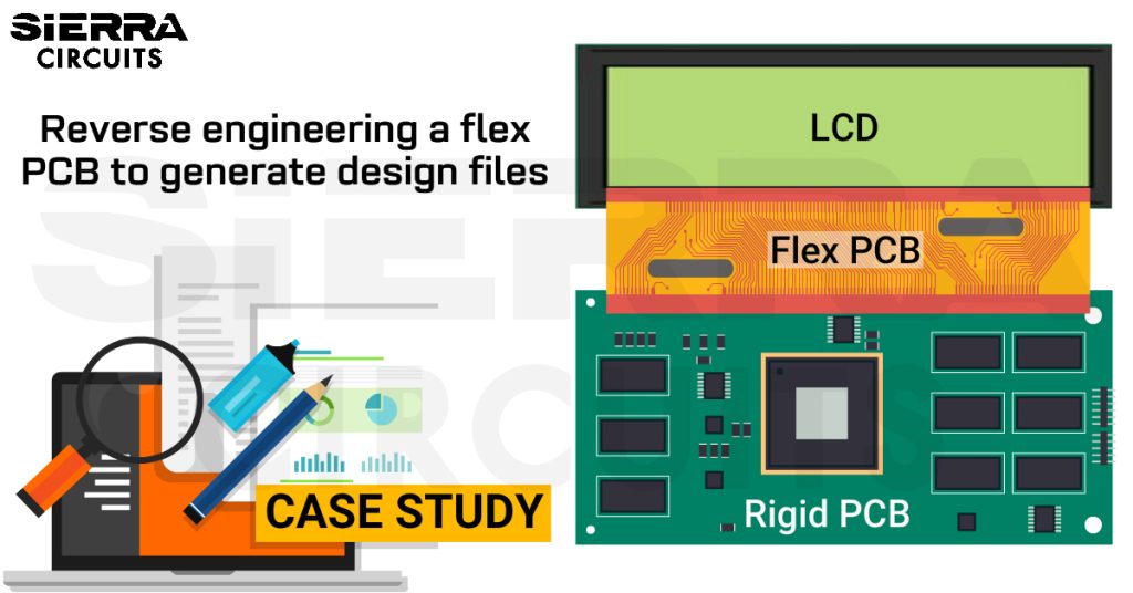
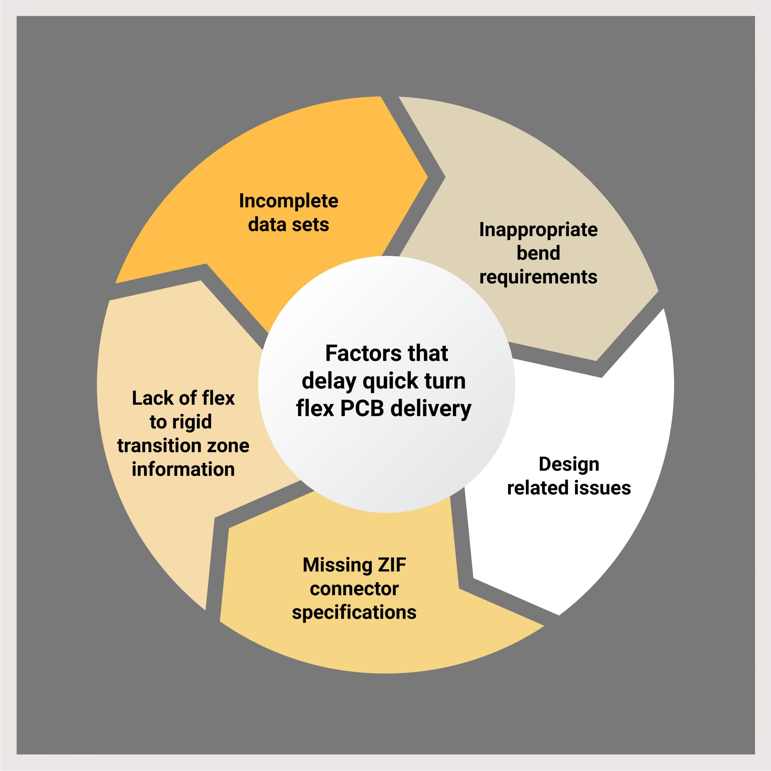
The production of flex circuit boards is rising at a rapid rate in response to the increased demand. Quick turn flex PCBs are in high demand and are put into production as soon as they are tested. Incomplete data sets and designs with technical issues are among the major obstacles that delay the quick turn lead time.
In order to get an electronic application to market as quickly as possible, the circuit design must be free of errors and violations. Incomplete data sets, inappropriate bend requirements, and lack of rigid to flex transition zone information can significantly increase the lead time of the flex board. The prominent issues are discussed in this article.
Data requirements for flex and rigid-flex PCB manufacturing
The initial step in the PCB fabrication process is to gather all the design data required by the manufacturer. These files will be used to create various layers and images of the circuit board. These are Gerber formatted files that trigger image formation on the fabrication film using a photoplotter. In addition to creating all the necessary layer images, these design files also provide drilling information for the board.
One of the prevalent factors that delay quick turn flex PCB delivery is providing design files with inadequate data sets. Data sets include Gerber/ODB++ files, fab drawing, spec sheet, and PCB stack-up.

The minimum data information requirements for placing an order for flex or rigid-flex circuit board are listed below.
Gerber files
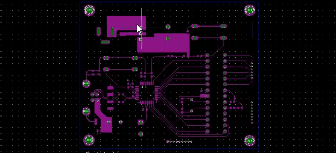
Gerber files are two-dimensional ASCII files that are commonly used by board designers and can be generated by most PCB design tools. These files are generated for each of the layers of the circuit board. To learn about exporting Gerber files, see how to export Gerber and other production files in KiCad. The below table lists various Gerber files required for board manufacturing.
| Number of files | File description |
|---|---|
| 1 | Top copper |
| 1 | Bottom copper |
| 1 | Top soldermask |
| 1 | Bottom soldermask |
| 1 | Top silkscreen |
| 1 | Bottom silkscreen |
| 1 | NC drill |
| 1 | Board outline |
| Depends on number of layers | Inner layers |
| 1 | Readme/images (optional) |
Common Gerber file mistakes to watch out for a quick turn flex PCB
- Missing drill files: Drill file comes with an extension “.DRL”. Ensure that the drill file is present in the Gerber data set.
- Missing solder mask layers: Verify if the top and bottom solder mask layers are present for multilayer boards.
- Missing or double outlines: Outlines display where the boards should be cut. Do not miss out this information in the Gerber file.
- Mismatching PCB size: The board dimension in the design file and the dimension in the placed order do not match sometimes. Verify that the selected dimensions correspond to the dimensions in the design file.
- Plated and non-plated holes are not clearly defined: It is important to understand how the CAD software differentiates plated and non plated holes. For example, Eagle software creates NPTH using the hole tool and PTHs are made by the via tool.
- Unclear layer nomenclature: In a 2-layered board, the top layer is usually labeled “TOP” while the bottom layer is labeled “BOTTOM.” However, boards with four or more layers may include inner layer designations such as power, ground, and so on. To minimize confusion, name the layers as L1, L2, L3, and so on to represent the order.
Missing information in the Gerber files can be one of the major factors that delay quick turn flex PCB delivery.
Formats of Gerber data
- 274D: It is the standard version of PCB design files produced by any CAM software. This file consists of commands and X/Y coordinates in ASCII format.
- 274X: It is a two-dimensional bi-level vector image description format used to manage numerically controlled machines such as raster-photoplotters. This file is commonly known as extended Gerber or X-Gerber. It is a superset of 274D standard Gerber. 274X contains a series of commands and coordinates to describe an image.
- ODB++: This file contains all of the information required to define a circuit board layer in a single directory. ODB++ file format provides a secure foundation for the required data. Designers can use this file to combine all of the essential data and run the appropriate checks for manufacturability and reliability.
- IPC-2581: It is a new file format that is gradually replacing earlier manufacturing file formats. This file includes manufacturing data needed for fabrication, assembly, and testing such as drill, netlist, etc. The advantage of IPC-2581 is that instead of generating numerous distinct files, PCB designers can simply export the design job as an IPC-2581 formatted file and send it to the CM.
Drill files
The drill file specifies the location, size, and the number of holes to be drilled on the board. The NC drill file can be used to accurately establish the location and size of all drill holes on the circuit board. Depending on the complexity of the circuit board wiring, the number of files created for the drill varies. Drills come in a variety of shapes and sizes, including through holes, blind vias, and buried vias.
PCB netlist
A netlist is a list of networks that determine the connectivity pattern of a bare circuit board. It provides information such as net names, pins, and XY coordinates.
Flex and rigid-flex fabrication instructions (fab notes)
The fab notes should contain all relevant information required by the board manufacturer:
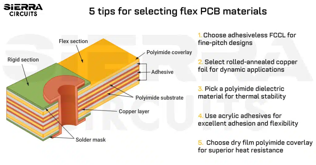
- Material stack-up that displays the copper weights, material specs, coverlay/solder mask requirements, and finished thickness with tolerances.
- IPC 6013 manufacturing class (class 1/2/3)
- Hole sizes with tolerances, and plating information
- Board dimensions and tolerances
- Hole or feature to edge dimensions
- Surface finish and silkscreen requirements
- Bend radius requirements
- ZIF connector specs
- Any additional requirements such as controlled impedance, stiffeners, type of adhesives, and so on.
Formats for fab notes
- Adobe Acrobat (.pdf)
- AutoCAD (.DWG or .DXF)
- Graphic file (.JPG, .GIF, .TIF, etc.)
- Array configurations – tab or scored preference
- Notes/read me files, and customer specifications

Design for Manufacturing Handbook
11 Chapters - 96 Pages - 90 Minute ReadWhat's Inside:
- Annular rings: avoid drill breakouts
- Vias: optimize your design
- Trace width and space: follow the best practices
- Solder mask and silkscreen: get the must-knows
Download Now
Bill of materials
A bill of materials (BOM) is a list of all the materials required to manufacture a product. Designers make use of BOMs to help the fabricator understand the components that they require during assembly. One of the main concerns with an incomplete component list is that some components may not be assembled onto the PCB or may be placed incorrectly. This will not only cause a delay in delivery, but it will also cost more money.
An accurate component list can help in avoiding a variety of issues that could cause delays in delivery and unnecessary expenses. To avoid these risks, make sure the BOM is up to date.
Inappropriate bend requirements
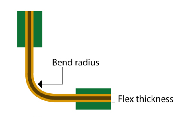
Sometimes, mechanical bend requirements will not be specified in the design. In a few cases, they are incorrectly defined to the point where it exceeds the physical capabilities of the materials. It’s a good idea to include information about where the bends will be placed and what will be the minimum bend radius. This will allow for a thorough design review, ensuring that the finished parts perform as expected.
According to IPC 2223C, bend requirements are divided into three groups. For each category, the minimum flex and rigid-flex bend capabilities are calculated as a multiple of the flex thickness.
- Flex to install: The flex circuit is bent into the desired shape before it goes into final assembly. Here, the flex circuit is not subjected to any additional major bend constraints.
| Number of layers | Minimum bend radius |
|---|---|
| 1 to 2 | 6 times the flex thickness |
| 3 or more layers | 12 times the flex thickness or more |
- Dynamic flex: A dynamic flex is a board that is regularly flexed (during the system operation). A dynamic board’s design needs to be more robust in nature, as flexing will occur on a regular basis and will need to withstand tens of thousands of bends.
| Number of layers | Minimum bend radius |
|---|---|
| Limited to 1 or 2 layers | 100 times the flex thickness |
- One-time crease: This type of flex circuit is bent/creased to a zero bend radius before being assembled to the final product. One-time crease flex designs are limited to 1 or 2 layers.
Common design issues in flex PCBs
While the data set creation procedure is similar to that of a rigid board, the IPC 2223 flex circuit design standard recommends a number of extra design rules. Below are a few design-related issues that delay the delivery of quick turn flex PCB.
- Unsupported component areas: Place the components in the rigidized area. Stiffeners are used to rigidize flex sections.
- Bend requirements in component areas: Placing components in the bend area could result in solder joint breakage.
- Vias or PTH in flex bend areas: Avoid having vias and PTHs in bend areas as they create mechanical stress when the circuit flexes. The hole plating may crack as a result of this. Vias or PTHs in flex bend areas require an additional drilling and plating process which not only increases the turnaround time but also adds to the overall cost. If the design requires vias/PTHs in the flex area consider the following points:
- Make sure vias are placed away for the bend locations.
- Request the CM to review the design and identify if there is any risk factor.
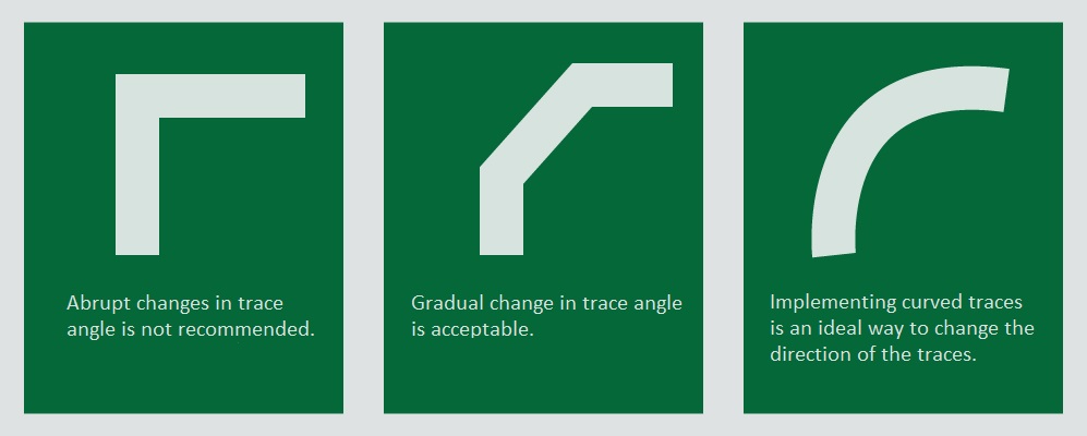
- 90-degree trace corners in flex areas: Avoid 90-degree bends if possible. Tighter bends increase the chance of circuit damage. The circuit will be safer if the bends are gradual.
To design better flex PCBs with Vern Solberg’s expert pre-layout tips, read flex PCB design guidelines part 1: pre-layout considerations.
Missing ZIF connector specifications
The ZIF connection (zero insertion force) is a connector attachment used in flexible PCBs that requires very little insertion force. It is very important to define the ZIF contacts, contact finger dimensions, coverlay opening dimensions, and stiffener thickness/dimensions in Gerber data and material stack-up. All of these components are required for a secure connection between the flex circuit and the ZIF connector. A flexible tail is not recognized as a ZIF contact without the necessary requirements in the Gerber data.
The following details should be present in the ZIF connector datasheet:
- Dimensions of the contact area.
- The thickness of the contact area (stiffening material + flex material + copper) including the tolerance. The industry standard is 0.3mm with a tolerance of ±0.05mm.
- Length of the stiffener.
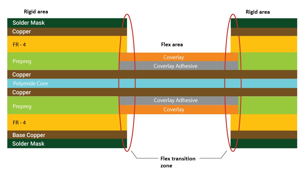
Flex transition zone
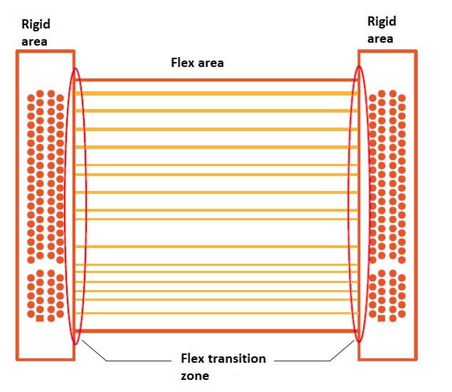
The rigid section outline where the layer structure switches from rigid to flex is known as the flex transition zone. A flex transition zone is created by extending the flex coverlays by a small distance into the rigid areas. This ensures a gapless transition between flex and rigid sections. Label the flex transition zone in the stack-up as shown below.
Flex transition zone design considerations
- Maintain a minimum clearance of 0.050” between PTH and the flex transition zone. This prevents any PTH from being drilled through the flex coverlays, ensuring plated through-hole reliability.
- Maintain a 0.025” minimum gap between the copper feature on the exterior layer and the flex transition zone. This provides enough space for accurate exterior layer imaging processing.
To learn more about solving via reliability issues in rigid-flex designs, see air gap construction method in rigid-flex PCBs.
It is very essential for a board designer to be aware of the factors that delay a flex board’s delivery time. The simplest method to avoid delays is to provide adequate data to your manufacturer and adhere to the standard design specifications. Let us know in the comments section if you have faced any other issues with your flex boards. You can download our design guide to understand more about flex design requirements.
Flex PCB Design Guide
10 Chapters - 39 Pages - 45 Minute ReadWhat's Inside:
- Calculating the bend radius
- Annular ring and via specifications
- Build your flex stack-up
- Controlled impedance for flex
- The fab and drawing requirements
Download Now
About Milan Yogendrappa : Milan Y is an electronics and communication engineer with over 6 years of experience in developing and editing technical articles related to PCB design, manufacturing, and assembly. He is currently the editor-in-chief at Sierra Circuits.