Related Categories — PCB Assembly » PCB Design » PCB Layout
PCB Design for Assembly Checklist: 9 Important Checks for Layout Engineers
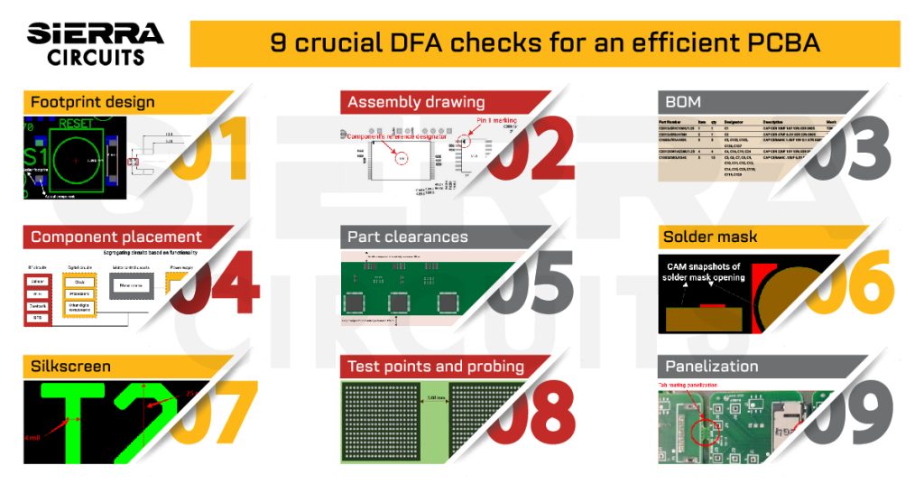
Here’s a PCB design for assembly checklist you can refer to before you proceed with the assembly process. This includes […]
PCB Assembly
How to Design PCBs for Data Centers and AI Servers
Designing PCBs for AI servers and hyperscale data center platforms requires architectures that support extreme routing density, high-speed ... more »
High Speed
How to Design an HDI PCB Stack-up
When designing an HDI PCB stack-up, you need to choose the right build-up architecture and define a via ... more »
HDI / Blind & Buried Vias
PCB Design for Assembly Checklist: 9 Important Checks for Layout Engineers
Here’s a PCB design for assembly checklist you can refer to before you proceed with the assembly process. ... more »
PCB Assembly
How to Design PCBs for Data Centers and AI Servers
Designing PCBs for AI servers and hyperscale data center platforms requires architectures that support extreme routing density, high-speed ... more »
High Speed
How to Design an HDI PCB Stack-up
When designing an HDI PCB stack-up, you need to choose the right build-up architecture and define a via ... more »
HDI / Blind & Buried Vias
How to Select and Place RF Components for PCB Designs
Choosing the right RF PCB components and placing them appropriately helps you avoid critical issues such as insertion ... more »
PCB Assembly
The Pros and Cons of Composite Amplifiers for PCB Designers
Several manufacturers are making serious efforts in widening the scope of composite amplifiers. The key features of these ... more »
PCB Design
How’s AI Transforming the Circuit Board Industry?
AI-assisted circuit board design is reshaping the schematic and layout creation process by recommending optimal part placement and ... more »
PCB Design
7 Tips and PCB Design Guidelines for EMI and EMC
Electromagnetic interference (EMI) is associated with every electronic device we use nowadays. If you turn on your radio ... more »
EMI and EMC
How to Become a PCB Designer in 2026
PCB designers are crucial in developing electronic devices, from smartphones to spacecraft. Circuit board design involves creating detailed ... more »
PCB Design
Sierra Circuits Receives Certificate of Appreciation from NASA’s Jet Propulsion Laboratory for Outstanding Support on AIRSAR-NG Mission
PRESS RELEASE Sunnyvale, CA — December 9th, 2025 — Sierra Circuits is honored to announce that we have ... more »
PCB Design
Fabrication, Procurement, & Assembly. PCBs fully assembled in as fast as 5 days.
- Bundled together in an entirely-online process
- Reviewed and tested by Engineers
- DFA & DFM Checks on every order
- Shipped from Silicon Valley in as fast as 5 days
Fabrication. Procurement & Assembly optional. Flexible and transparent for advanced creators.
- Rigid PCBs, built to IPC-6012 Class 2 Specs
- 2 mil (0.002″) trace / space
- DFM Checks on every order
- 24-hour turn-times available
Complex technology, with a dedicated CAM Engineer. Stack-up assistance included.
- Complex PCB requirements
- Mil-Spec & Class 3 with HDI Features
- Blind & Buried Vias
- Flex & Rigid-Flex boards


