


Contents

On-demand webinar
How Good is My Shield? An Introduction to Transfer Impedance and Shielding Effectiveness
by Karen Burnham
Imagine you’re designing PCB transmission lines for a high-speed application. You’ve routed critical interfaces like PCIe and USB 3.0; however, during validation, some unexpected eye diagram distortions start surfacing.
After hours of debugging, you realize the issue arises from discontinuities in transmission line impedance. At this stage, redesigning the signal lines is not just tedious; it’s pricey and delays your entire project.
In this article, you’ll learn the root causes of signal attenuation, the impact of impedance variations, and proven design techniques to maintain uniform impedance in high-speed applications.
Highlights:
When designing transmission lines for your circuit boards:
- Use impedance matching techniques like series or parallel termination to reduce signal reflections and maintain integrity.
- Route differential pairs and clock lines using serpentine routing to align signal timing and avoid skew.
- Taper down the traces gradually if changes in trace width are required.
- Maintain a uniform trace width to ensure consistent impedance.
Watch the full webinar here: How to design PCB transmission lines with controlled impedance.
Importance of controlled impedance in PCB transmission lines
Here are 4 reasons why you need to maintain uniform impedance in high-speed traces:
1. Prevents signal reflections
If the transmission line impedance is inconsistent, it causes signal reflections. These reflected signals interfere with incoming signals, leading to PCB ringing, jitter, and data corruption.
Moreover, signal reflections increase EMI, which can cause the PCB to fail EMC tests. Interference might lead to catastrophic failures in critical applications like medical or automotive PCBs.
For example, in a PCIe or USB 3.0 interface, even minor impedance mismatches can result in lost packets, causing retransmissions, reduced throughput, or even system crashes.
2. Minimizes the risk of skews
High-speed signals often rely on precise timing relationships. A change in impedance can cause variations in signal propagation speed, resulting in timing skews and setup/hold violations.
Especially in DDR memory designs or serial buses, even a few picoseconds of timing mismatch can create functional errors.
Thus, controlled impedance ensures every bit arrives on time, maintaining data integrity and synchronization.
3. Facilitates heat dissipation
Impedance mismatches cause parts of the signal energy to be reflected rather than absorbed by the load. This wasted energy manifests as heat and reduces the system’s power efficiency.
By ensuring controlled impedance, we maximize energy transfer and minimize unnecessary heat buildup, making the circuit more thermally and electrically efficient.
4. Reduces signal attenuation
As signals travel over longer distances, they naturally attenuate. Inconsistent impedance matching accelerates this loss, causing signal amplitude to drop below detectable thresholds.
PCB transmission lines with uniform impedance minimize loss, helping you maintain strong and clean signal levels from source to destination, even in longer traces.
Download our design guide to learn more about PCB transmission lines.

PCB Transmission Line eBook
5 Chapters - 20 Pages - 25 Minute ReadWhat's Inside:
- What is a PCB transmission line
- Signal speed and propagation delay
- Critical length, controlled impedance and rise/fall time
- Analyzing a PCB transmission line
Download Now
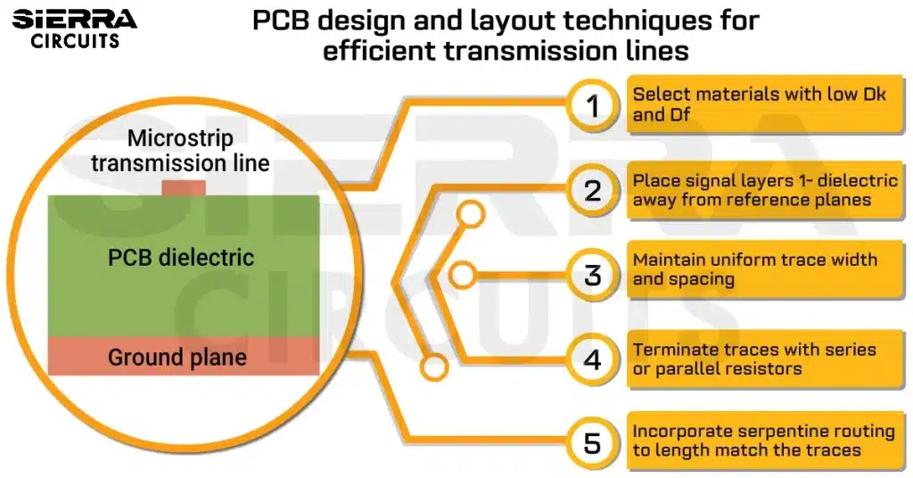
5 design and layout techniques for designing PCB transmission lines
1. Select the right high-speed PCB laminates and low-profile copper
At high frequencies, dielectric materials can contribute significantly to signal loss through leakage currents and molecular polarization. To reduce these losses:
- Select substrates with high volume resistivity (e.g., >10⁷ Ω-cm) to limit high leakage currents in PCBs.
- Opt for a low dielectric constant (Dk < 4) material to increase signal propagation speed and reduce parasitic capacitance.
- Choose materials with a low dissipation factor (Df < 0.005) to minimize dielectric loss, where signal energy is converted to heat.
Materials like PTFE (Teflon) and Rogers laminates (e.g., RO4003C) meet these criteria and are widely used in RF circuit boards.
As frequency increases, current tends to travel along the outer surface of the conductor (skin effect). This reduces the effective cross-sectional area for current flow and increases conductor resistance.
To reduce these losses, use low-profile copper foils such as hyper-very low profile (HVLP), ultra-low profile (ULP), or reverse-treated copper.
These foils have smoother surfaces (roughness <0.5 µm), which reduce scattering losses and improve signal integrity, especially above 1 GHz.
Smoother copper reduces insertion loss, making it ideal for 5G PCB designs.
At high frequencies, current concentrates near the surface of conductors, reducing the effective cross-sectional area and increasing resistance. To reduce skin effect losses at high frequencies, employ various low-profile copper foils, such as hyper-very low profile, reverse-treated foil, and ultra-low profile.

Download our eBook to learn how to select the right materials for your high-speed PCBs.
High-Speed Material Design Guide
6 Chapters - 19 Pages - 30 Minute ReadWhat's Inside:
- Importance of choosing the right material for your high-speed design
- Parameters that affect material selection
- Effect of dielectric constituents on your circuit board
- Characteristics of high-speed materials
- Effect of resin content and glass weave structure on your PCB
Download Now
2. Place the signal layers one dielectric away from the reference planes
PCB stack-up design plays a major role in the performance of transmission lines. Position signal layers just one dielectric layer away from their corresponding reference planes (either ground or power). This setup helps suppress noise by providing a low-impedance return path, which reduces loop inductance and electromagnetic radiation.
For RF designs, route high-frequency traces and place components on the outer layers of the board. External layers (top or bottom) are ideal for radio frequency traces like antennas or filters, which typically form microstrip or coplanar waveguide structures. In these cases, the transmission line impedance depends on factors like trace width, dielectric constant, and board thickness.
Using outer layers also makes it easier to tune impedance, place RF components like ICs and matching networks, and run signal integrity tests.
Group signal layers based on their operating frequencies. For example, in one of the designs, our PCB design engineers kept a 2.4 GHz RF signal on the top layer and a 100 MHz digital signal on the bottom layer. This separation helped reduce interference and ensured cleaner signal paths.

At Sierra Circuits, we can build PCBs with ±5% impedance tolerance. We add impedance test coupons to each panel and validate the impedance to ensure it matches your requirements. These test coupons replicate the trace structure and layer stack-up of the actual PCB.

See our controlled impedance capabilities to learn more.
3. Maintain uniform trace width
A consistent trace width is essential for maintaining a stable transmission line impedance. Sudden changes in trace width can cause impedance discontinuities, which lead to signal reflections and power loss.
If you need to change the trace width, do it gradually. Use a linear or exponential taper to transition between widths smoothly. This helps minimize reflections and maintain signal integrity.

Consider using thicker copper (e.g., 2 oz/ft² instead of 1 oz/ft²) for high-power and high-current traces. Thicker traces reduce DC resistance and improve current-carrying capacity. While high-frequency signals are affected by the skin effect (which confines current to the trace surface), increased surface area from thicker traces still helps reduce effective resistance and prevents overheating.
To minimize crosstalk, maintain a spacing of 3W to 5W between adjacent traces (where W is the trace width). This separation helps reduce unwanted electromagnetic coupling, especially in high-frequency designs.

Lastly, ensure that your trace impedance matches the connector impedance. For example, if you’re using a 50 Ω RF connector (like an SMA), the trace should also be 50 Ω. Impedance matching ensures maximum signal transfer and minimizes reflections or distortions at the interface.
To learn how to minimize impedance discontinuity, see how to limit impedance discontinuity and signal reflection in PCB transmission lines.
4. Terminate traces with series or parallel resistors
To minimize signal reflections in high-speed PCB designs, terminate transmission lines using resistors. Two common methods are series termination and parallel termination.
In series termination, a resistor is placed between the driver and the transmission line, close to the driver. The goal is to make the total impedance at the driver side (driver impedance + resistor) match the trace impedance.

For example, if the driver impedance is 23 Ω and the trace impedance is 50 Ω, you can use a 27 Ω series resistor near the driver to achieve impedance matching. This helps reduce overshoot and ringing by damping the initial signal.
In parallel termination, a resistor is placed at the receiver end of the transmission line, in parallel with the input. This resistor absorbs any reflected signals that reach the end of the line, preventing them from bouncing back and causing interference. Depending on the receiver’s design, the termination resistor may be tied to ground or to a supply voltage (e.g., Vcc) to maintain proper logic levels.

Each method has advantages, and the choice depends on your design’s signal speed, power budget, and IC requirements.
For more, read 5 PCB trace termination techniques to reduce signal reflections.
5. Incorporate serpentine routing to align signal timing
Serpentine routing (also known as meandering) is a technique used to match trace lengths for timing-critical signals. It involves routing a trace in a back-and-forth (snake-like) pattern to add extra length without significantly affecting signal integrity.
Implement this technique when:
- Differential pairs need to maintain equal electrical length to avoid timing skew.
- Clock and data lines in synchronous buses must stay aligned to meet setup and hold time requirements.
- One signal in a pair or group is physically shorter and needs length compensation to match the others.

Best practices for serpentine routing:
- Maintain at least 3W spacing between adjacent segments of the meander to avoid unwanted capacitive coupling.
- Use gentle curves instead of sharp corners to reduce impedance discontinuities.
- Avoid routing serpentine traces near sensitive areas, such as power planes or noisy switching circuits.
While serpentine routing is a useful technique, avoid overusing it. Excessive meandering can introduce additional inductance or capacitance, degrading the signal quality. Aim to match lengths within your design’s specified tolerance (typically within ±10 mil for high-speed signals).

Common types of signal losses that occur in PCB layouts
Signal attenuation is an inherent phenomenon that degrades signal quality as it propagates through a transmission line. Thoroughly understanding the various losses and implementing strategies to mitigate them is essential for ensuring the system’s overall reliability.
Insertion loss is the total reduction in signal power as it moves through a transmission line, compared to the original signal launched at the source. It is typically expressed in decibels, with higher dB values indicating greater loss.

Why it matters:
- Excessive insertion loss reduces the signal-to-noise ratio (SNR), making signals more susceptible to errors.
- It might cause jitters, eye diagram closure, and limit the achievable maximum data rate.
- It increases the bit error rate (BER), a critical specification in communication standards like Ethernet, PCIe, or USB.
Insertion loss is caused due to:
- Conductor loss
- Dielectric loss
- Radiation loss
1. Conductor loss
Conductor loss refers to the decrease in signal strength as it travels through a conductor. At low frequencies, current flows uniformly throughout the entire cross-section of the copper trace, and the effective cross-sectional area available for current flow is significant. This keeps the resistance of the conductor relatively low.
However, as frequency increases, the skin effect becomes significant. Due to electromagnetic principles, current tends to be pushed toward the conductor’s outer surface (skin). The effective area through which the current can flow shrinks, and it becomes limited to a thin layer at the conductor’s surface, known as the skin depth.
Since resistance is inversely proportional to the cross-sectional area (R ∝ 1/A), the shrinking of the effective area leads to a higher resistance at high frequencies.
This increase in resistance directly contributes to conductor loss in high-speed transmission lines. As resistance rises:
- More signal energy is dissipated as heat.
- Signal amplitude decreases over distance.
- The system becomes more prone to noise and distortion.
- More power is required to maintain adequate signal levels, increasing thermal stress.

2. Dielectric loss
It occurs when the signal’s electric field interacts with the molecular dipoles in the PCB material, causing some of the signal’s energy to convert into heat.
Dielectric loss depends on two key material properties:
- Dielectric constant (Dk): Measures how much the material slows down an electric field.
- Dissipation Factor (Df ): Measures how much energy is lost as heat.
Higher Dk and Df values result in greater energy absorption, increasing signal loss. As frequency increases, dielectric loss becomes more dominant than conductor loss.

3. Radiation loss
Radiation loss refers to the phenomenon where electromagnetic energy is emitted into free space from the traces. As signal frequency increases, the wavelength decreases (since wavelength λ = c/f, where c is the speed of light and f is frequency). When the wavelength becomes comparable to the physical dimensions of the trace (e.g., trace length or width), the trace can behave like an antenna.
Uncontrolled radiation from traces can generate EMI, which affects nearby electronic devices. The radiated electromagnetic waves can couple into other circuits, antennas, or traces, inducing unwanted currents or voltages.
Due to radiation loss, the signal amplitude might be reduced at the receiver, which degrades the signal-to-noise ratio. In power amplifiers or RF systems, radiation loss reduces the power delivered to the load.

Unlike conduction losses (in copper) or radiation losses (into free space), leakage loss occurs due to the imperfect insulating properties of the dielectric material.
Dielectric materials have a finite resistivity and can conduct small leakage currents when subjected to an electric field. This becomes critical at high frequencies, where the electric field changes rapidly. The leakage current results in energy dissipation within the dielectric. This is often modeled as a shunt conductance (G) in the transmission line model. The loss is proportional to the dielectric’s conductivity (inverse of resistivity) and the square of the applied voltage.
At low frequencies (<100 MHz), leakage loss is typically negligible because the dielectric’s resistivity is high, and the leakage current is small. Whereas, at very high frequencies, the rapid oscillation of the electric field increases the effective conductivity of the dielectric due to polarization effects and dielectric relaxation. This makes leakage currents more significant.
To understand the mechanism of signal losses, see losses in PCB transmission lines.
Loss comparison among stripline, microstrip, and CPW

For more, see our article, what is the difference between microstrip and striplines in PCBs?.
Impact of solder mask on insertion loss
In high-speed PCB design, the interaction between the signal’s electromagnetic fields and the surrounding materials is critical in determining signal quality and losses.
A stripline transmission line is embedded between two dielectric layers, with ground planes placed above and below the signal trace. This setup fully contains the electromagnetic fields within a controlled dielectric environment.
As a result, stripline structures do not interact with external materials like solder masks, and thus do not suffer significant additional dielectric losses due to solder mask coatings.
In contrast, microstrip and coplanar waveguide transmission lines are located on the outer layers of the PCB. The signal trace is exposed to the air. Since microstrips and CPWs have fields that extend into the surrounding environment, solder mask applied over the trace will interact with a portion of the signal’s electromagnetic field.

The signal no longer experiences the substrate’s Dk; instead, it sees a combination of dielectric constant (air, substrate, and solder mask).
Solder masks typically have higher dissipation factors (< 0.025) compared to high-frequency substrate materials (< 0.005). This higher Df causes increased dielectric losses, leading to greater insertion loss and degraded signal integrity, especially at high frequencies.
Hence, it is better to leave high-frequency signal traces uncovered through solder mask openings or mask clearance.
Every detail, such as material selection, stack-up planning, trace routing, and termination strategies, is crucial in maintaining transmission line impedance. By proactively designing for uniform impedance and understanding the conductor, dielectric, and radiation losses, you can deliver robust, high-speed boards that meet today’s stringent reliability standards.
Start implementing these techniques today, and elevate your PCB designs to new heights of reliability and speed!
Have questions about your high-speed printed board design? Post your queries on SierraConnect. Our PCB experts will answer them.

About Poulomi Ghosh : Poulomi is a microwave engineer specializing in EMI, EMC, RF, and high-speed electronics. As a senior technical writer at Sierra Circuits, she creates advanced engineering articles and webinars for hardware engineers and PCB designers.


Start the discussion at sierraconnect.protoexpress.com