Contents

On-demand webinar
How Good is My Shield? An Introduction to Transfer Impedance and Shielding Effectiveness
by Karen Burnham
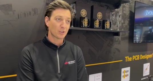
Stephen Slater during DesignCon-2022 gave us a wonderful chance to talk about his views on next-gen memory and signal integrity in high-speed boards. Watch the video.
Stephen Slater works as a product manager in the High-Speed Digital Simulation Technology at Keysight. His expertise lies in high-speed SerDes channel simulations, DDR simulations, and electromagnetic simulations for PCB applications.
What are key design aspects to consider for next-gen memory applications like DDR5?
Stephen Slater: I think we are at a tipping point in the last couple of years. In Keysight, we have been working along with semiconductor vendors, and getting into simulating DDR5, but not with many system design houses. Last year, Intel came out with a new chipset, Alder Lake, that supports DDR5. Even at DesignCon, we have seen papers where people have built DDR5 systems. It is a turning point, and I think there are going to be many more designs starting this year.
But, for DDR4, going into DDR5 is a big technology change. One of the things we have to be careful with is that you can not leverage the DDR4 designs and just expect it to work for DDR5. It is a redesign. At that point, the signal integrity engineer needs to start with a good pre-layout design. What pre-layout enables you to do is put together transmission lines and vias, parameterize them and adjust them, and explore the design space to find out if you are going to have enough design margin.
That is quite critical for DDR5 because there is a possibility that you could end up with a completely closed eye at the input to the receiver. It is one of the biggest changes from DDR4 to DDR5. They have got equalization now on the receiver. The signal coming in could be completely closed out, but after equalization, it recovers the signal and we have a good link. The simulation tools have changed and the way you go about testing and measuring has changed. For simulation, we have now moved away from using traditional spice simulation. We use more channel simulation to look at DDR5, where you can see the effects of the equalization.
When it comes to measurement, they have built a new set of interposes, which try to keep the crosstalk at a minimum. Keysight’s scopes themselves are low-noise scopes. We recover the signal even if it is closed. You can apply equalization inside the scope to open the eye up and make sure that you can receive the signal properly. Probably, that is the biggest change in the technology, but it is exciting and has the possibility of being twice as fast as the fastest speed rate for DDR4, once we get to the updates.
Can you brief us on critical issues involved in the PCB layout for DDR5?
Stephen: One of the biggest changes, I think, is that as we start to move faster, we need to be more careful about crosstalk. These signals are going to connect to the pads in the BGA pin field that the device would rest upon. You are going to have more crosstalk in that pin field. The number of ground vias and their location is going to be important.
You can’t always get away from the additional crosstalk there is going to be, but at least you need to be able to simulate it to estimate how much impact crosstalk is going to be. The other aspect is about the length matching. So DDR5 is a parallel bus, just like DDR4 was. It is critical that you take into account how much transmission line length is inside the package of the device, and you are given that information upfront.
When you go to board layout, work with the package lengths and then make sure that the rest of the signals you create are still time aligned at the end. But we use meanders and serpentines. The electrical length of those and the physical length is slightly different. Even though you have laid it out, you do want to be able to verify with an EM simulator to make sure that the signals are going to be time-aligned as they enter into the system.

A PCB with multi-gigabit high-speed links requires careful design. Could you recommend some design choices to improve signal integrity at 16 Gbps and beyond?
Stephen: We move away from memory now and talk about high-speed serial, let’s say 16 Gbps. It is like a PCI express gen-four type of link. One of the key things was we had is a survey with some PCB designers. We asked them how many of them optimize the vias that they use. Two-thirds said that they don’t. They have a good standard via model that they use for all the high-speed traces, the designs. This is an opportunity when you get to 16 Gbps and even faster. There is an opportunity to take a look at adjusting the antipad clearance size, which would adjust the capacitance of the via, then the numbers and the location of the ground stitching vias.
The more ground stitching vias you add, you will get lower inductance. If you bring them in closer to the signal vias, you will end up getting less inductance. This is a balance between how much capacitance and inductance you need. You are trying to balance them so that you end up with your target desired impedance for the via that would match the signal trace coming into it. I have got a paper where we talk about that. We can get 50 millivolts extra eye height by paying more careful attention to the transmission line impedance, matching it to the via, and coming up with a good, more optimal design.
Signal Integrity eBook
6 Chapters - 53 Pages - 60 Minute ReadWhat's Inside:
- Impedance discontinuities
- Crosstalk
- Reflections, ringing, overshoot and undershoot
- Via stubs
Download Now
Designing high-speed boards poses many challenges in terms of signal integrity. How does it impact the system performance?
Stephen: Let’s come back to that example of our PCI express-gen 4. Taking that design to something like gen-5, I may design this PCB but it is not the whole system. I take this add-in card and put it into a mainboard and the signal gets from this board to the receiver, but I don’t design the mainboard and the connector. So how do you make sure that the thing that you design is going to work?
That is the way Keysight is trying to solve. We have created a library of PCI express-gen-5 reference channels. You can do some budgeting. You have got your design, but then I have got a model for a connector, the mainboard, and the package things which I don’t control. But if I can put them into my system simulation, I can simulate the whole system together and make sure that my design is going to work, whichever configuration it needs to. Because sometimes it is just a single add-in card into the mainboard. It could easily be a single board, mainboard, and then another add-in card. You need to check for all these different CRNs of how you design the main network.
High-Speed PCB Design Guide
8 Chapters - 115 Pages - 150 Minute ReadWhat's Inside:
- Explanations of signal integrity issues
- Understanding transmission lines and controlled impedance
- Selection process of high-speed PCB materials
- High-speed layout guidelines
Download Now
Can you mention some of the key tools that Keysight offers that will help analyze designs accurately and predict their performance?
Stephen: Our primary flagship product is Pathwave ADS. It is an advanced design system with a very big design environment inside it. You have got a lot of useful tools. If you are designing vias, we use a via designer, it is a three-dimensional view, but everything is parameterized. You type in the width and spacing of the different clearance holes and pads, and it will change it and extract the model. Then you can use that in your schematic simulation. For things like memory design, the product inside of ADS is called Memory Designer. It is nice and easy to remember. That is what you use for being able to do the pre-layout and then the full system design for memory. When you talk about EMI extraction, if signal integrity, then it is SI pro, and if it is power integrity, we use a PI pro.
One brand new thing we have at the show is for power integrity. We have a new conducted EMI analysis. That is very interesting because usually that is something that takes a long time to set up. This is why engineers shy away from doing the analysis. You can go from a DC analysis, you have set up, and then just copy it over to this newly conducted EMI analysis. Everyone needs to be checking that they are going to pass the conducted EMI specifications, and this enables you a chance to fix the problems before you get further down the path and build a prototype.
About Poulomi Ghosh : Poulomi is a microwave engineer specializing in EMI, EMC, RF, and high-speed electronics. As a senior technical writer at Sierra Circuits, she creates advanced engineering articles and webinars for hardware engineers and PCB designers.


