


Contents
To successfully design a flexible PCB, it is important for the designers to have a basic understanding of the flex drawing requirements.
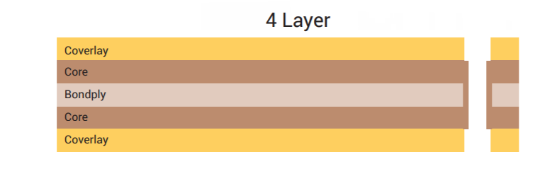
Flex PCB stackup construction and layer order
PCB stackup differentiates between rigid layers and flexible layers in the PCB. The flexible PCB stackup drawing will give the thickness of each layer including the copper thicknesses of the conductive layers. This should also show which layers are rigid material and which layers are flexible material including copper weights. Sierra Circuits can assist you in designing your flex stackup.

Dimensional drawing and tolerances
The dimensional drawing identifies a number of critical measurements for the PCB design. It should define the rigid to flex interfaces (where these two types of materials meet). The typical outline tolerance is +/- 0.010″.
The dimensional drawing of a flexible PCB design provides the following information:
- PCB stiffeners’ location and dimensions
- Thicknesses of each section of the PCB and the materials to be used
- Static or dynamic flex type during operation of the circuit. A PCB that flexes a maximum of 20 times is called a semi-static flex PCB. A PCB that is regularly flexed and twisted is called a dynamic flex PCB. Printers use dynamic flex PCBs as the circuit flexes throughout the operation of the printer.
- Locations where the board rarely flex and frequently flex.
Flex PCB materials to be used
Selecting the right PCB materials for your flex PCB design is very important as it can impact the overall performance of the flex PCB. Before selection begins, we need to make sure material characteristics fit your specific board requirements and end application. It is vital to mention which type of materials to be used for your flex PCB manufacturing process. The flex PCB materials include:
- Flexible dielectric material
- Conductors (copper type)
- PCB Stiffeners

Specifications
The PCB manufacturer expects the following range of specific details from the designer.
- Class type (class 1, class 2, class 3), wiring type, and installation use requirements
- Flexible copper clad material to be used
- The cover coat material
- Maximum board thickness
- The minimum size of plated through holes
- Electrical test requirements
- Color of coverlay
- Color of silkscreen
- Board markings such as part number, version, and company logo
- Packaging and shipping needs
- Minimum conductor width and spacing
- Special packaging requirements (if any)
Drill symbol chart
The drill symbol chart indicates all of the finished hole sizes, as well as the hole size tolerance, for your circuit board design. To learn more about PCB drilling read PCB Drilling Explained: The Do’s and the Dont’s. The drill symbol chart summarizes the drill holes’ information present on the board. An example of a drill symbol chart is shown below. The standard finished hole size is +/- 0.003″ but this is never assumed, so this measurement must be stated on your design drawing.
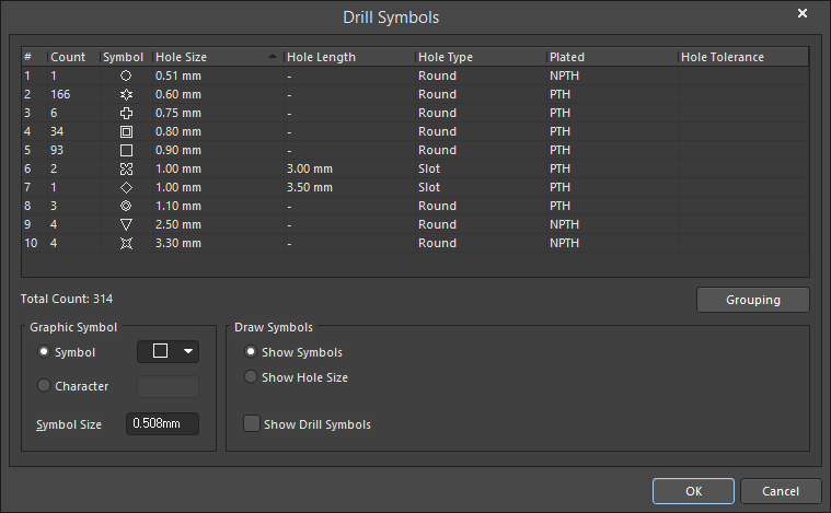
Each of the symbols represents a drill size. The other columns in the chart provide information like hole shape, and hole type (Via or non-plated).
Flexibility (Bend radius)
The flexibility of a flex PCB is determined by the bend radius of the flex material used. Bend radius is the minimum angle the flex region can bend. The below illustration helps us to understand the concept of the bend radius.
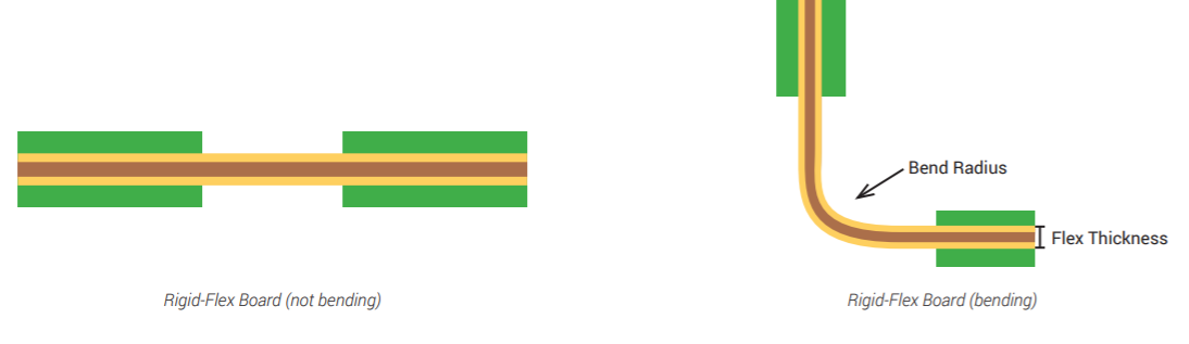
Knowing the number of times your flex PCB will bend is crucial in your design. If a PCB is bent more times than the design allows for, then the copper will begin to stretch and crack.
The bend radius depends on the number of layers and the type of material used in the flex.
To know more about flex design considerations read our article Avoiding Common Flexible PCB Errors and Designing for Success.
Plating requirements
Plating the through-holes or vias is a requirement for multilayer PCBs. It is very important to mention the type of plating that your flex PCB requires. The available types of plating are:
- Panel plating
- Pattern plating
- Pads only plating
Panel plating: This method of plating deposits copper on the entire panel. This type of plating is generally performed before circuit imaging.
Pattern plating: This type of plating deposits copper on the selected areas of your flex PCB.
Pads only plating: It is a type of pattern plating. An image resists covers the entire panel leaving the pads capturing the vias. As a result, only the vias and exposed pads get plated.
In Sierra Circuits, we use a selective plating process “pads only plate” to plate copper in the through-holes. In order to accomplish this, we drill the flexible copper clad dielectric material and then image the “pads plate” image around the drilled holes at (drilled diameter) D + 0.003” or better. After plating the holes with approximately .001” of copper we image again with the finished circuitry pattern and the etch the desired pattern. An additional D + 0.014” of the pad is needed for this etching process, which puts our minimum pad size on double-sided flexible products at a drilled diameter + .017.” These pads should always be as large as your design will allow.
Testing requirements
Physical and electrical testing requirements should be mentioned (test type and frequency). When specifying testing the designer should consider the needs very carefully. Over specifying the test requirements might increase the overall circuit cost. The testing of a PCB include:
- Dimensional checks
- Electrical continuity
- Inductance
- Capacitance
- Ionic cleanliness
- Flexibility
- Plating thickness
- Insulation resistance
For more, read IPC standard and guidelines for testing flex PCBs
Marking requirements
The manufacturers would like the designers to specify the type of ink to be used for various board markings like serial numbering, component mounting location, stiffeners/cover locations, and panel-based marking. The types of ink include:
- Durable white ink
- Traditional epoxy ink handstamp
When we design a flexible PCB it is very crucial for us to provide the vital information(drawing requirements) to the manufacturers as this information helps them to fabricate the flexible PCB as per the designer’s expectation without any time delay.
Flex PCB Design Guide
10 Chapters - 39 Pages - 45 Minute ReadWhat's Inside:
- Calculating the bend radius
- Annular ring and via specifications
- Build your flex stack-up
- Controlled impedance for flex
- The fab and drawing requirements
Download Now
About Amit Bahl : Amit Bahl, widely recognized as the PCB Guy, earned his Bachelor of Science in Engineering from UCLA. He is currently the Chief Revenue Officer at Sierra Circuits, where he continues to lead efforts to simplify the PCB design journey and support designers and engineers in creating high-quality boards.


