


Contents
Flexible PCB design errors can be avoided by ensuring the manufacturability of your design and by communicating with your supplier.
Depending on the application, a higher manufacturing cost will cut the overall costs in the long run. Pay close attention to the complexity of the flexible PCB application as well as the capabilities and recommendations of your supplier.
Give your supplier an idea of what you want to do, and make sure they can manufacture your PCB design.
In this article, we will be looking into the following aspects of the flexible PCB design:
1. Flexibility and number of layers of flex PCBs
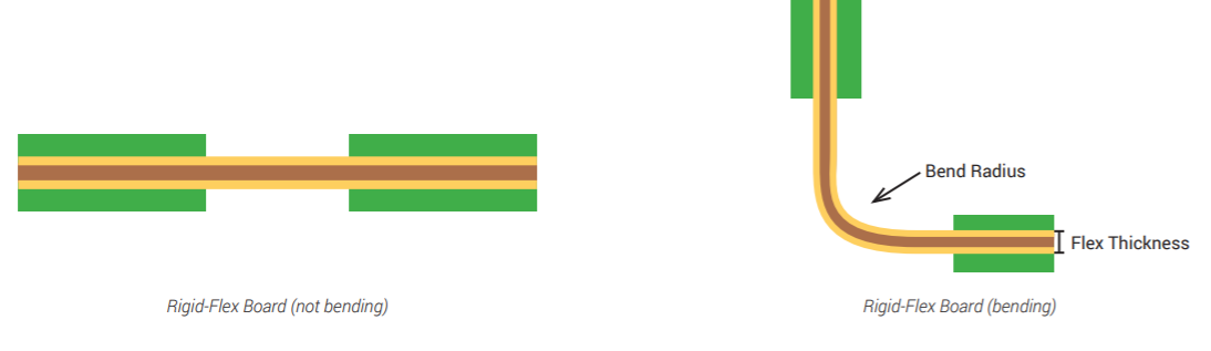
Knowing the number of times your flexible PCB will bend is crucial to your design. If a PCB is bent more times than the design allows for, the copper will begin to stretch and crack. Bend radius is the minimum amount the flex area can bend.
If a PCB flexes a maximum of 20 times, then it is called a semi-static flex PCB. If a PCB is regularly flexed and twisted, it is called a dynamic flexible PCB.
Bend radius can be calculated using the below table:
| Number of layers | Bend radius (mils/mm) |
|---|---|
| 1 (single-sided) | Flex thickness x 6 |
| 2 (double-sided) | Flex thickness x 12 |
| Multi-layer | Flex thickness x 24 |
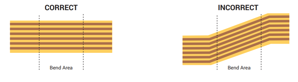
Consider the following points to limit the flexible PCB errors in the bend areas:
- Avoid 90-degree bends. Tighter bends increase circuit damage.
- Always measure the bend radius from the inside surface of the bend.
- Place conductors smaller than 10 mils inside the neutral bend axis, as they tolerate compression better than stretching.
- Avoid plated through-holes within the bend area.
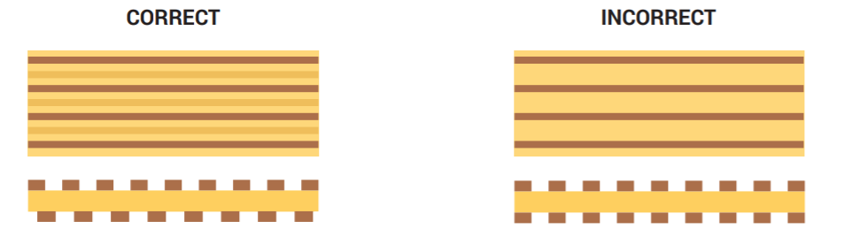
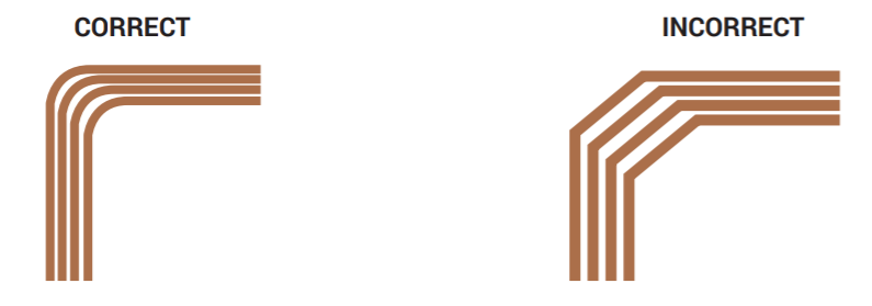
2. Flexible PCB traces
The performance and longevity of a flexible PCB can be directly attributed to the layout of the circuitry. Signals should never be routed at sharp angles. Sierra Circuits recommends the largest radius possible for your design. In addition, I-beaming will not only reduce the flexibility of your circuit, it will increase stress contributing to the thinning of copper circuits at the bend radius.
When designing multi-layer flexible PCBs, stagger traces on the front and back.
Use curved traces instead of traces with corners
Rigid-flex PCBs brings down the overall electronic product assembly cost. To know more about it read our article Rigid-Flex Cuts Electronic Product Assembly Costs
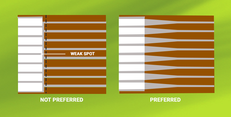
3. Trace width
In a flexible PCB, a trace entering a pad forms a weak spot in which the copper might get fatigued over a point of time. It is always recommended to taper down the pads towards (as shown below) the end in which they are connected to the traces.
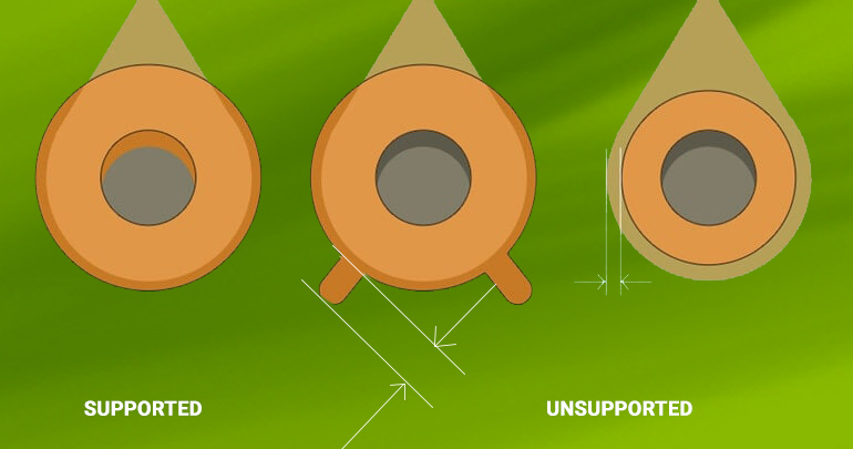
4. Support for pads on flexible PCBs
On a flex circuit, copper is prone to be detached from the substrate due to the bending of the flex circuit. It is vital to provide mechanical support for the exposed copper. The through-hole plating in the vias inherently provides mechanical support to the vias in the flex region. For this reason, additional through-hole plating of up to 1.5 mils is recommended for rigid-flex and flex circuits. Usually, SMT pads and non-plated through-holes are referred to as unsupported, and they require additional measures to prevent detachment.
5. What is the difference between coverlay and solder mask?
Coverlay is the combination of Kapton and adhesive whereas solder mask is liquid-based. One of the largest differences between coverlay and solder mask is their state. Coverlay is a solid material made of plastic polyimides, or plastic with adhesive, while the solder mask is a liquid. Keep coverlay dam (prevents the flow of molten solder on one pad to a neighboring pad) sizes a minimum of 10 mils; solder mask dam sizes should be a minimum of 4 mils to avoid flexible PCB errors.
For coverlay, the trace to mask opening can be as close as 3 mils. For the solder mask, 3 mils could lead to misregistration or undercut issues (relating to the imaging of the solder mask). Sierra Circuits suggests maintaining a distance of at least 4 mils for solder mask.
Generally, coverlay is used on the flex sections and the solder mask is used on the rigid section of the PCB. If you would like to use coverlay for your entire rigid-flex board, then window opening or gang opening should be present. Also, please note that coverlay cannot be used on the tight pitch components.
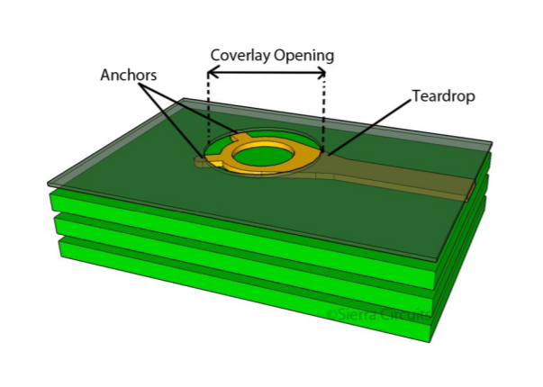
6. Flex vias and via keep-out areas
Vias are at a greater risk of getting peeled off from the flex layers. Consider the following points to reduce the flexible PCB errors associated with vias.
- Make annular rings as large as possible.
- Vias should be tear-dropped. Teardrops can reduce potential stress concentration points on the PCB.
- Adding tabs or anchors to vias, as shown below, will also help prevent peeling.
Via locations:
- Vias are not reliable in areas that will bend.
- In a dynamic application, flexed vias can crack very quickly.
- Vias are okay over a stiffener, but vias just off the edge of a stiffener are at risk of cracking.
- Vias should be placed at least 20 mils away from the rigid-flex/flex interface.
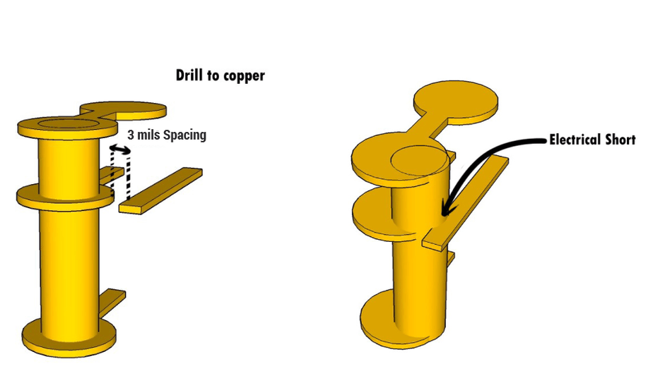
7. Drill-to-copper
When designing flexible products it is crucial to keep drill to copper in mind. That is, the distance between a hole (via or non-plated) and a copper trace. The flexible dielectric materials that are used to manufacture flex products are not as dimensionally stable as a standard rigid material. This material moves, shrinks, and contracts during the manufacturing processes which makes drill to copper critical to a successful product. Drill to copper should be of a minimum of 8 mils to reduce errors in the flex PCB.
8. Controlled impedance traces in flex PCBs
Impedance or commonly called characteristic impedance of a PCB trace is a measure of how much the circuit impedes the flow of current. It is like resistance, but it also takes into account the effects of capacitance and inductance. Impedance is measured in ohms.

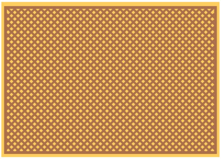
A cross-hatched reference plane has a significant impact on the impedance control in flex designs. Since cross-hatching means the plane is no longer solid copper but has a significant percentage of copper removed from it, the plane no longer provides 100% shielding to the signal traces. As such, the controlled impedance of the signal traces increases.
To learn more about flex design guidelines for manufacturing, watch our webinar Flex PCB Design Guidelines for Manufacturing.
9. What are PCB stiffeners? Why are they used in flex PCB?

A PCB stiffener isn’t an electrical piece of the PCB, yet assumes the job of offering mechanical support. It is an additional mechanical piece that provides mechanical support to the flex PCB during the assembly and application.
We utilize a stiffener when we have to harden a specific area in the flex circuit. First, we need to understand that the PCB stiffener is not an integral part of the electrical circuit board design. This will not let the circuit bend and will protect the integrity of the part’s solder joint. Stiffeners support the specific areas of the board that contain SMT and/or PTH components.
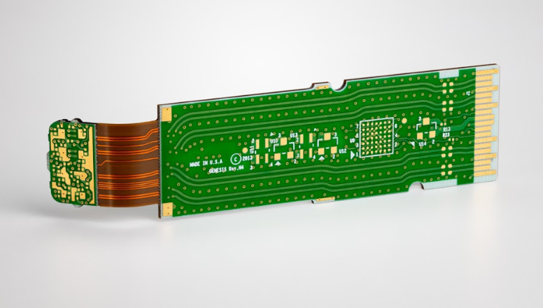
10. Rigid-flex PCB stack-up construction and layer order
Rigid-flex stack-up differentiates between rigid layers and flexible layers in the PCB. The flexible PCB stack-up drawing will give the thickness of each layer including the copper thicknesses of the conductive layers. This should also show which layers are rigid material and which layers are flexible material including copper weights. Sierra Circuits can assist you in designing your flex stack-up. The below image shows a sample 6 layer rigid-flex stackup.
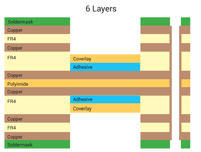

Sample 6 layer rigid-flex stackup. To know more about flex drawing requirements read our article 9 Drawing Requirements for Flex PCB. Flex PCBs offer numerous advantages over their rigid counterpart. Read our article The Advantages of Flex PCBs And Their Applications to know more about it.
The design of flexible PCBs requires several additional considerations. Keeping things simple in terms of the design and the PCB materials can help you steer clear of some of the flexible PCB errors we outlined here. Usage of standard materials is recommended when possible because they have proven track records when it comes to their throughputs and yields.
Getting a great flex PCB starts with finding a top-notch PCB supplier like Sierra Circuits. Check out our main flex PCB page to find out more, and also be sure to take a look at our flex PCB design guide.
Flex PCB Design Guide
10 Chapters - 39 Pages - 45 Minute ReadWhat's Inside:
- Calculating the bend radius
- Annular ring and via specifications
- Build your flex stack-up
- Controlled impedance for flex
- The fab and drawing requirements
Download Now
About Amit Bahl : Amit Bahl, widely recognized as the PCB Guy, earned his Bachelor of Science in Engineering from UCLA. He is currently the Chief Revenue Officer at Sierra Circuits, where he continues to lead efforts to simplify the PCB design journey and support designers and engineers in creating high-quality boards.


