Contents
In her presentation at the Winter 2019 IPC Designers Council Silicon Valley, Natasha Baker, founder & CEO of SnapEDA, discusses the challenges of creating and maintaining high-quality PCB libraries, as well as the difficulties that engineers face when designing circuit boards.
https://protoexpress.wistia.com/medias/uyx5p7b5bx#
Natasha Baker is the Founder of SnapEDA, a search engine for PCB libraries and other models needed to design circuit boards, used by a million electronics designers worldwide. She holds a Bachelor’s degree in Applied Science in Electrical Engineering from the University of Toronto. With a decade of experience pertaining to the PCB industry, she has learned common pitfalls that engineers make when designing electronics.
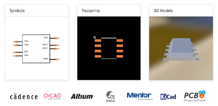
SnapEDA is used by over a million professional engineers from around the world to build circuit boards faster. It provides free PCB footprints, schematic symbols, and 3D models for millions of electronic components, allowing engineers to focus on design and innovation, rather than library creation.
Why should you build a quality PCB library?
When designing a PCB, each electronic component requires a symbol for the schematic capture, which describes pin functions, mappings and types, and a PCB footprint, to ensure that the component is soldered to the board correctly. Additionally, 3D models are also generally used by engineers to check clearances between their PCBs and their mechanical casings.
High-quality libraries can be difficult to get right, but are an essential element of the PCB design process, because they ensure:
- Proper and reliable manufacturing
- Other CAD tool features function properly (ex: ERC and DRC checks)
- Consistency, which makes designs readable and reusable
Building a good PCB library comes with a number of challenges and difficulties, as discussed in Natasha Baker’s presentation. First of all, it’s a very detail-oriented process, where a high level of precision is necessary for each pin, pad, and part. Additionally, there is a lack of consistency in how datasheets are created, which can inadvertent errors during their interpretation.
Lack of standards and industry alignment is another major challenge in building high-quality PCB libraries. Additionally, users or companies have specific preferences or requirements. Up until recently, most companies had their own standards, but nowadays we’re observing a shift in the industry towards creating and using more industry standards.
Finally, a library’s importance is often underestimated and overlooked. All companies know it is important to have footprints that manufacture well, but in practice, prioritizing library maintenance over other critical tasks can be challenging.
In her talk, Natasha Baker also discusses common errors engineers make when creating PCB designs. Such mistakes include pin mapping issues, pad dimension errors, silkscreen overlapping exposed copper, and wrong outline dimensions or misinterpretations of the component dimensions. On top of those, there are some less common mistakes that even highly experienced engineers can make, such as using mirrored top/bottom views, wrong or misinterpreted datasheets, wrong centroids, wrong component zero orientation, and more.

To avoid those, verifying the library before a design goes to manufacturing is an important part of the work process for every design team, regardless of the library’s origin (whether it’s from the component manufacturer, an existing library that the company had created, or an external library from a third-party website), and there are a few crucial steps to follow. These steps can be briefly summarized, as follows: defining a strong verification process and maintaining and enforcing detailed checklists.
In order to help engineers overcome the challenges that they’re facing when designing circuit boards and verifying their designs, SnapEDA provides a number of tools. Those include supporting a wide array of design formats, providing the possibility to automatically build parts by using computer vision and optical character recognition and also to request the footprint & symbol of a specific component (if it’s not already in the library) instantly.
In conclusion, libraries, although often overlooked, are indispensable for reliable manufacturing, readability, and to enable ERC, and DRC checks. Implementing a strong verification process is essential for good PCB design. A number of tools exist to help engineers design faster and be more efficient and productive.
7 PCB Libraries Questions Answered by Natasha Baker
Which standards should I use for my PCB libraries? What factors will affect the manufacturability of my final PCB? What are the common errors that I need to be extra wary of when I define my libraries to prevent unneeded PCB prototype iterations? These are some of the many question’s PCB designers ask before starting their designs. We decided to address these issues to make life easier for PCB designers. So, we sat down with Natasha Baker and asked a few questions faced by PCB designers during the selection of PCB libraries.
Sierra Circuits: Why do PCB libraries matter?
Natasha Baker: We need PCB libraries to ensure proper manufacturing. PCB libraries are so important because they affect the manufacturability and yield of your design. For instance, an improper pin-out in a design can render your PCB completely dysfunctional, resulting in time-consuming re-work, or even unnecessary board respins. Further, if pads are off by even a fraction of a millimeter, it can lead to improper soldering. This is why spending time to ensure your libraries are well-defined is crucial.
PCB libraries don’t always get the attention they deserve within the industry. However, I think that’s short-sighted because they’re the backbone of any electronics design.
SC: Which are the frequently followed standards when creating PCB libraries?
NB: One of the most popular standardization bodies working on creating standards for footprints – or land patterns – is the IPC. The latest standard for surface mount components is the IPC-7351B, and the release of an updated version of that standard is imminent. IPC-7351 standards define all aspects of the footprints – including aspects like the solder mask, solder paste, and courtyard. Organizations like IEEE also cover symbol standards, especially for common discrete components.
SC: What are the common mistakes made by designers during the PCB component selection?
NB: Pin mapping issues are probably the most basic mistake made by designers. Mapping the symbol pins to the footprint pins is extremely tedious – especially on a high-pin count part like an FGPA – so it’s not too surprising. But this is usually one of the first mistakes to burn an engineer.
Another frequent issue we see amongst newer engineers is placing silkscreen over the copper pads, which can lead to bad solder joints.
In terms of more seasoned engineers, the most common issue by far is misinterpreting a component’s bottom view as being its top view. When this happens, the component gets “mirrored”. There are some hacks to fix this issue (in some cases the component can be flipped on the board and its legs bent backward), but obviously, this is a pretty unpleasant one to run into.
SC: Do we need to update PCB libraries with examples?
NB: The standards change, and that means things like recommendations on the copper lands, or even the default orientation of a footprint can change (which matters because it’s required for the pick-and-place machine). So yes, staying on top of the latest industry standards is a good practice.
SC: Is it important to verify PCB libraries?
NB: Yes, whether you get a library from a website (such as SnapEDA or a component vendor’s website) or your team creates it themselves, it is crucial to go through a standard set of checks as part of your DFM process, for the reasons mentioned earlier. The cost of an error is high, and because libraries are so detail-oriented, it is important to always verify the details.

SC: What is the approach of larger organizations in regard to PCB libraries?
NB: Times are changing rapidly in the PCB industry. It used to be mainly large corporations designing electronics, and they had dedicated librarians to support the engineers. But as design teams have gotten smaller, we’ve seen a huge surge in engineers looking for ready-to-use libraries. It’s amazing how much things have changed in just 5 years.
SC: How do you stand out from others?
NB: I’d say that engineers really need to try it to experience the magic. SnapEDA saves engineers so much time, and we keep adding new features to improve their lives. Some examples, are our computer-vision symbol builder InstaBuild (www.snapeda.com/instabuild), our computer-vision symbol builder, and InstaPart (www.snapeda.com/instapart), our 24-hour request service for PCB libraries.
To find free symbols, footprints, and 3D models for your designs, visit the SnapEDA website.
You can book a meeting with our experts or call us at +1 (800) 763-7503.

Quote and order your circuit boards online with our Turnkey PRO tools in just a few minutes.