


Contents

On-demand webinar
How Good is My Shield? An Introduction to Transfer Impedance and Shielding Effectiveness
by Karen Burnham
PCB assembly requires certain files to provide a basic idea about the component positions, orientation, and courtyard information of each and every layer. These include Gerber/ODB++, centroid, BOM, assembly drawings, and so on.
All the files for board manufacturing and assembly are generated using design and documentation tools. The procedure to generate PCB assembly files depends on the design software used.
Complete assembly documentation provides a basic insight into all procedures and inspection techniques required to yield the end product. Therefore, it is necessary to know about these files and their generation procedures. We will discuss in detail about these files, in this article.
What design files are needed for PCB assembly?
As mentioned above, among the files required for assembly, the most important ones are Gerber/ODB++, centroid file, assembly drawings, and BOM. As a PCB design engineer, if you do not communicate necessary information to your contract manufacturer (CM) through these files, then several errors may arise. These include mismatch of component quantities, absence of pin 1 and polarity markings, missing orientation indicators, footprints, and so on.
PCB assembly files are important because of the following reasons:
- Provide effective communication between the vendor and customer for proper board population.
- The absence of board assembly files may lead to errors related to the position and orientation of components and result in high repair costs.
- Some data that is not obtained from silkscreen are gathered from these files.
- Lack of important information like polarity markings or position of through-hole components during manual soldering causes discrepancies.
To know more about the common design pitfalls leading to PCBA errors, see our article 6 design mistakes that lead to PCB assembly errors.
How to generate circuit board assembly files
For the assembly process, manufacturing data is also required. Let us explore the different file types and the methods to generate PCB assembly files.
Gerber files
Gerber files are helpful in both circuit board manufacturing and assembly processes. These files are generated for each and every layer in the stack-up. Apart from the layer information, there are other data incorporated in these files. All the layers are specifically mentioned like top, bottom, solder mask top/bottom, assembly top/bottom, silkscreen top/bottom, fab layer, and so on.
In addition to the layer descriptions, details regarding aperture definitions and data generated for board etching, also form a part of these files. RS-274D and RS-274X are the most common types of PCB file formats. RS-274D is called standard Gerber and RS-274X is known as extended Gerber. Gerber X2 is another version that supports file extensions like .top and .bot.
ODB++ files impart all the vital information along with the layer details. Hence, by opting for these files, you will be able to accommodate stack-up details, placement information, bill of materials, and fabrication requirements. Thus a single file provides abundant information as compared to Gerber.
It is critical to look for the common problems related to Gerber files, such as multiple aperture lists, design files mismatch, etc. This assures the utmost accuracy of the files.

Design for Manufacturing Handbook
11 Chapters - 96 Pages - 90 Minute ReadWhat's Inside:
- Annular rings: avoid drill breakouts
- Vias: optimize your design
- Trace width and space: follow the best practices
- Solder mask and silkscreen: get the must-knows
Download Now
Generating Gerber files
EDA tools available today help generate Gerber files by merely selecting the required layers. Here are procedures for KiCAD, Allegro, and Altium Designer tools.
KiCad
- Click on the plot icon in the toolbar. In the pop-up window, choose Gerber as the Plot format and the required Output directory.
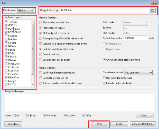
- Next, check off all the required layers under Included layers option.
- Remember to select the layers like top paste, bottom paste, forward silk, bottom silk, solder mask top, solder mask bottom as well.
- Check off your specific requirements under General options.
- You can uncheck Plot footprint values option.
- Under Gerber options, select Use Protel filename extensions and then click Plot.
- The files will be generated and saved in the selected output folder.
For more details about generating Gerber, drill file, netlist, BOM, and other production files in KiCad, read how to export Gerber and other production files in KiCad.

Allegro
- Go to Manufacture > Artwork in the top menu bar.
- In pop-up window, click on Apertures > Edit > Edit Aperture station > Auto > Without rotation, and hit OK.
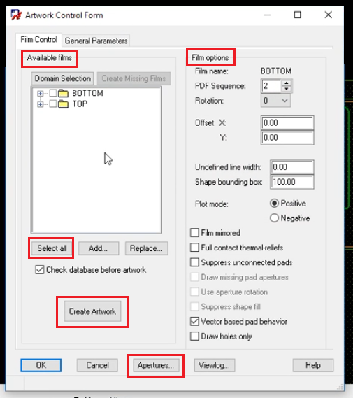
- Choose all the required layers under the Available films section. Right-click on the folder and select Add manual to access more layers.
- Other parameters to be set come under Film options. Specify the Undefined line width as required (4mils for example). You can check off Suppress unconnected pads option.
- Now click Select all under the Available films section and choose Create artwork.
Get an in-depth understanding of generating Gerber, netlist, NC drill file, and BOM using Allegro in our tutorial how to export Gerber and design files in Allegro.
Altium Designer
- Open File > Fabrication Outputs > Gerber Files.
- In the pop-up window, there are 5 tabs.
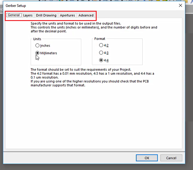
- Under the General tab, set the units for measurement and number format.
- The layers tab allows you to select the required layers that should appear in the file. There will be two columns. The left one specifies which particular layer to print and the right one allows to select the layers that are commonly printed on all other layers.
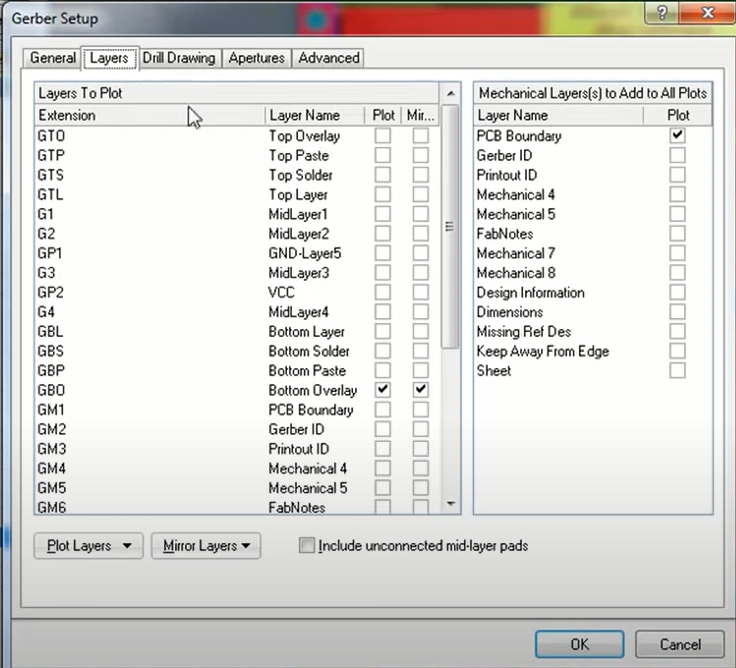
- All the board drilling configurations such as symbols, drawing plots, and drawing guides are done in the Drill drawing tab.
- Under the Apertures tab, there is an option to activate Embedded apertures that provide the output Gerber in RS274X format.
- The next tab is called Advanced. Here, choose the Separate file per layer check box under Batch mode and click Ok to generate separate files for each layer.
- Gerber files are generated at the selected output folder.
Learn more about exporting Gerber, NC drill files, BOM, and ODB++ in detail here how to export Gerber and production files in Altium Designer.
Centroid file
Centroid files describe the X-Y location, orientation, reference designator, layer details, and package information of all the components. These files are also known as X-Y data files or pick and place files. Few of the design tools have the capability to automatically generate centroid files. In some tools, you have to modify existing data to generate these files.
How to create centroid files
In this section, like earlier, we will discuss the procedure to create these files using the three most commonly used design tools.
KiCad
- Follow the path File > Fabrication outputs > Footprint position (.pos) file.
- In the pop-up window, choose the output directory.
- Under the Format section, select the format (ASCII or CSV) and units.
- In the Files section, you have the option to choose between a single file for all layers or separate files for the top and bottom layers. Select the right one and click Generate position file.
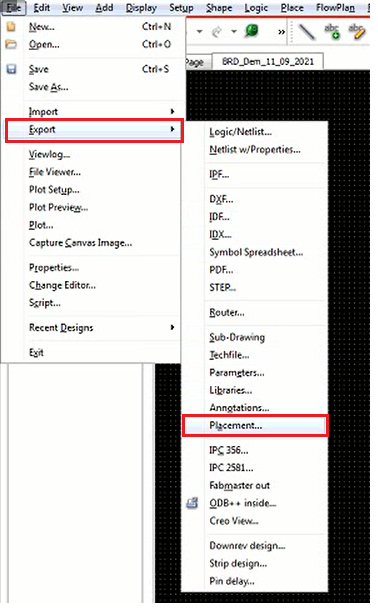
Allegro
- First, the position of components is obtained from Files > Export > Placement. In the pop-up window, name the file and choose where the origin should be, and click Export. This gives a file with rotation, X-Y coordinates, and footprint names of the components.
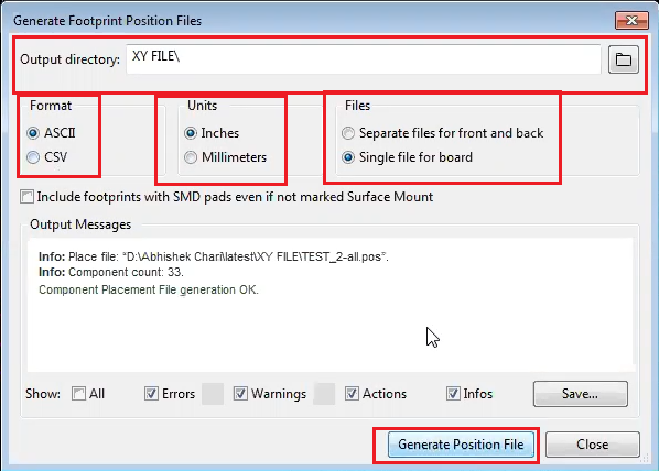
Altium Designer
- Select File > Assembly outputs > Generates pick and place files.
- A window appears with all the parameters that are available and lets you choose the ones needed.
Bill of materials (BOM)
BOM includes all the information about the components to be assembled on the circuit board.
BOM generation
The procedures involved to produce a BOM using the design tools are as follows:
KiCad
- Choose the “Generate bill of materials” icon at the top ( alternatively File > Fabrication outputs > BOM).
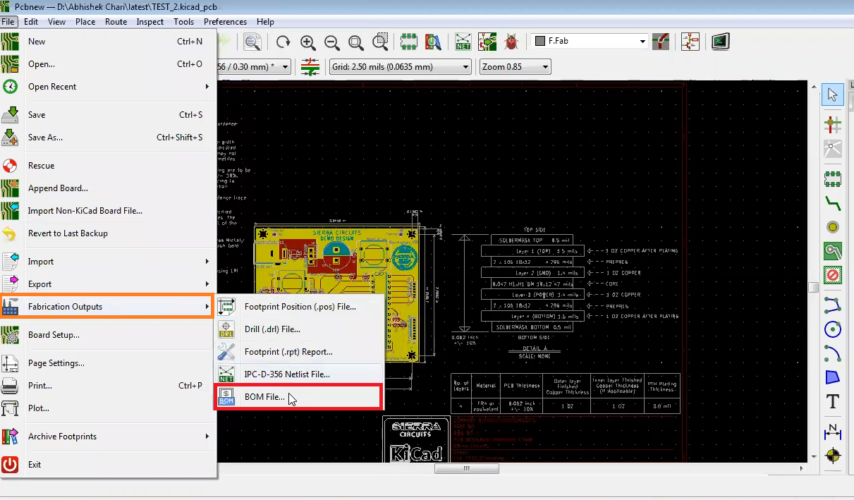
- In the pop-up window, different options for bill of materials are available under the BOM plugins section. Choose the one that suits your requirement.
Allegro
- Select the schematic from the project files. Right-click and choose Edit object properties.
- In the next window, select the properties that need to be on the bill of materials and remove the unwanted ones. Once done, close the window.
- Go back to the project, select the schematic, and choose Tools > Bill of materials.
- In the pop-up, two columns named Headers and Combined property string will be present.
- In Headers, add all the columns that have been introduced in the Edit Object Properties earlier. The format is “t” followed by the name.
- The same has to be added in the Combined property string as well. The format is “t{new property}”. Make sure that the names are exactly the same as those given in the Edit Object Properties option earlier (including spaces and uppercase).
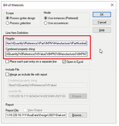
- Check-off the Open in Excel box and click OK.
Altium Designer
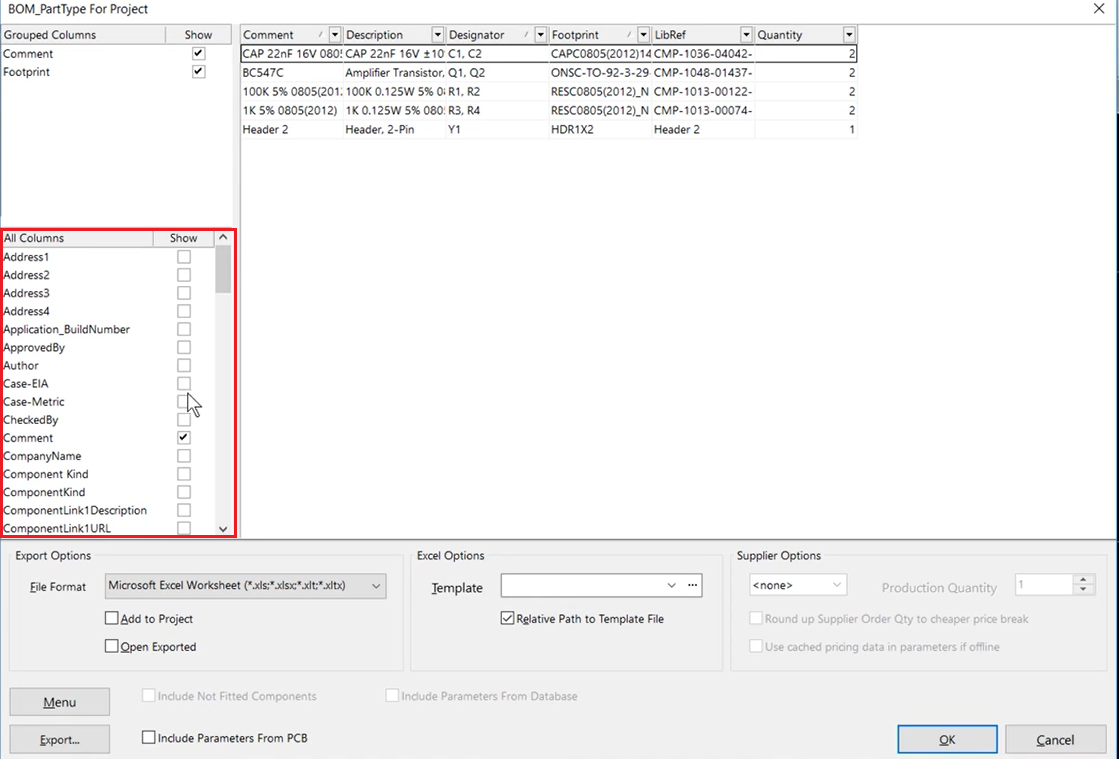
- Go to Reports > Bill of materials. In the new window, select the Columns tab.
- Customize the BOM by adding or removing the required properties.
- Click Export to save the BOM file with the preferred name.
Assembly drawing
Assembly drawings are a set of documents that describe how the components are placed on the outer layers of a PCB. The assembly team and inspection team of technicians refer to these documents to get an idea about the accuracy of component placement. An assembly drawing includes the following:
- Pictorial representation: An outline of the board showing the component locations and corresponding reference designators.
- Assembly details: Included when there is a space restriction in the pictorial to explain densely packed regions or small parts.
- Assembly notes: Help the assemblers with information like the designation of primary side, mounting instructions, soldering instructions, specialized assembly methods, height restrictions of the board, cable orientation, etc.
How to generate assembly drawing
Here we will discuss the methods required to generate assembly drawings.
KiCad
- Go to Plot > PDF > select F.Fab and B.Fab layers (assembly layers in KiCad).
- In the available options, check-off “Plot border and title block”, “Plot footprint values”, “Plot footprint references”, “Force plotting of invisible values/refs”, “Exclude pads from silkscreen” and uncheck the “Exclude PCB edge layer from other layers” option.
Allegro
There are two methods here.
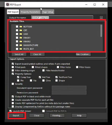
- Go to File > Export > PDF. In the window, choose the required layer whose layout is needed, under Available Films.
- These films can be customized under Manufacturing > Artwork.
- Select the fab layer, click on Export to generate a PDF of the fab layer, and similarly, choose generate the PDF of the assembly layer.
Alternative method:
- Select File > Plot and save as PDF. Whichever options are turned on and are visible on the board at the time of plotting will be printed as a PDF.
Altium Designer
- In the .pcbdoc file, go to File > Assembly Outputs > Assembly Drawings.
- A preview of the assembly file will appear. Click on the Print button below and save it as a PDF file.
Proper documentation is a necessity when it comes to quoting, assembly, and inspection. The inspection report involves documenting various process parameters according to the type of test like AOI, X-ray, etc. If you want to learn about all the inspection details, read our post on the PCB assembly inspection report format. There are so many assembly stages dependent on these files and hence their presence is vital. We hope that the PCB assembly files types and generation procedures are clear from this article. If you have any queries, please reach out to us in the comments section.

PCB Design for Assembly Handbook
6 Chapters - 50 Pages - 70 Minute ReadWhat's Inside:
- Recommended layout for components
- Common PCB assembly defects
- Factors that impact the cost of the PCB assembly, including:
- Component packages
- Board assembly volumes
Download Now


