Contents
Documentation is a pivotal component of the product lifecycle. PCB assembly inspection report is an essential element of the documentation package of circuit boards. The format of this report should be accurate and understandable.
What does PCB assembly inspection mean?
Transforming the design files into a physical form that accurately represents the design purpose involves two stages: manufacturing and assembly. For a circuit board to comply with all requirements, it is vital to perform inspections to validate the results and review the board’s quality. Assured quality is one of the many benefits of choosing turnkey PCB manufacturing and assembly from a single facility for your designs. PCB assembly inspection reports include all the relevant data from various inspection tests executed on the board.
Several tests are available that fulfill the quality standards such as visual, manual, and X-ray inspection. Each test has its specification levels that range from measuring different parameters to finding missing parameters. All the details from such tests are documented in inspection reports to verify a defect-free product. This approach guarantees continuous improvement in the process.

Board assembly inspection checklist
There is no standard format for the assembly inspection checklist. It can vary from industry to industry. However, some industries like automotive and aerospace require it in a particular format due to strict documentation norms.
Some must-have attributes in the inspection report are:
- Inspected components and subassemblies
- Testing and type of inspections performed
- Reports on inspection findings and the corrective actions taken to resolve any defects
- Inspection equipment/method
- The locations and dates of the inspections

PCB Design for Assembly Handbook
6 Chapters - 50 Pages - 70 Minute ReadWhat's Inside:
- Recommended layout for components
- Common PCB assembly defects
- Factors that impact the cost of the PCB assembly, including:
- Component packages
- Board assembly volumes
Download Now
Parameters for different types of tests carried out on a populated circuit board
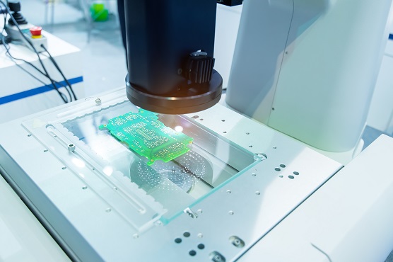
Parameters are the constraints that define the scope of the process. Here, it indicates the inspection scope for a specific process type. For example, a manual inspection can only examine the overview of a board up to the maximum resolution permitted by the naked eye. It cannot detect hidden defects; X-ray imaging is the only way to find them.
It is essential to understand and consider these parameters while preparing the inspection report. Categorizing the parameters under a proper process is also vital. Let’s see all the inspection tests and their respective parameters:
Manual inspection
Manual inspection or visual inspection is the simplest method of inspecting a circuit board. To conduct this test, one can examine the board either with the naked eye or through a magnifying glass. It includes the comparison of the board with the design documents to ensure that the specifications are met. Types of defects vary according to the kind of board and the components mounted on it.

The checklist for manual inspection includes the following elements:
- Verifying the board’s warpage.
- Measuring the dimensions of an assembly according to the customer’s specifications.
- Confirming component solder joints are free of solder bridges, open solder, cold solder, etc. as per IPC or customer-defined workmanship.
- Inspecting PCB surface for pits, scratches, dents, pinholes, and other defects.
- Ensuring there is no component damage and no incorrect component mounting orientation.
- Other requirements as specified.
However, the scope of this method is limited. There are certain drawbacks.
- Manual inspection is time-consuming and expensive. It does not assure high quality.
- With miniaturization and technological advancements, the board requires high-level techniques for inspection.
Read our post on 6 types of electronic component failures in boards to understand various defects such as warpage, creep, brittle fracture, etc.
AOI inspection
Automated optical inspection is a widely used method for inspecting devices under test (DUT) to examine various surface feature defects such as open circuits, short circuits, etc. This technique is used in circuit board manufacturing as well as assembly. This system comprises illumination, a machine vision camera, and processing software.
A machine vision camera scans the circuit board and looks for defects. Since the process requires proper illumination, the AOI machine uses LED lighting that provides optimum lighting for accurate verification of different parts. The processing software employs two methods: the golden board standard and algorithm-based programming.
AOI inspection detects errors such as:
- Solder shorts, and open circuits
- Components with incorrect marking, missing, or skewed
- Misplaced chips, or chip-orientation defects
- Violations of component spacing.
- Offsets and polarity of components
- Excessive and insufficient solder joints
- Flipped parts
- Defects in specific areas
AOI inspection differs based upon the 2-D and 3-D evaluating machines.
Board manufacturers can detect coplanarity with 3D inspection on height-sensitive devices without a problem, although shadows may cause issues in some board layouts.

X-ray inspection
X-ray inspection or automated X-ray inspection is the most reliable tool for finding invisible errors in circuit boards with ICs (CSP: chip-scale package) and BGAs. It can scan and detect large voids and cracks. This method can access internal geometries and structural compositions without causing any damage. The test is performed in the same way as AOI by capturing images.
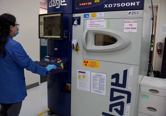
X-ray inspection system identifies voids within solder joints that are not visible to AOI.
This system can determine faults like:
- Soldering defects: Solder bridges, open solder, insufficient solder, excess solder, and poor solder quality
- Component defects: Lifted lead, missing components, and misplaced components
The X-ray inspection method is beneficial when BGA, CSP, and similar packages are used, as the error detection in such cases exceeds the capabilities of AOI.
Refer to our post on 8 common errors in surface mount technology (SMT) to learn more about soldering defects like bridges, open solder, etc.
In-circuit test
In-circuit test (ICT) involves testing populated PCBs to examine their resistance, capacitance, shorts, opens, and other electrical quantities to ensure a sound fabrication. It is possible to conduct this test with either a bed of nails fixture or a flying probe tester.
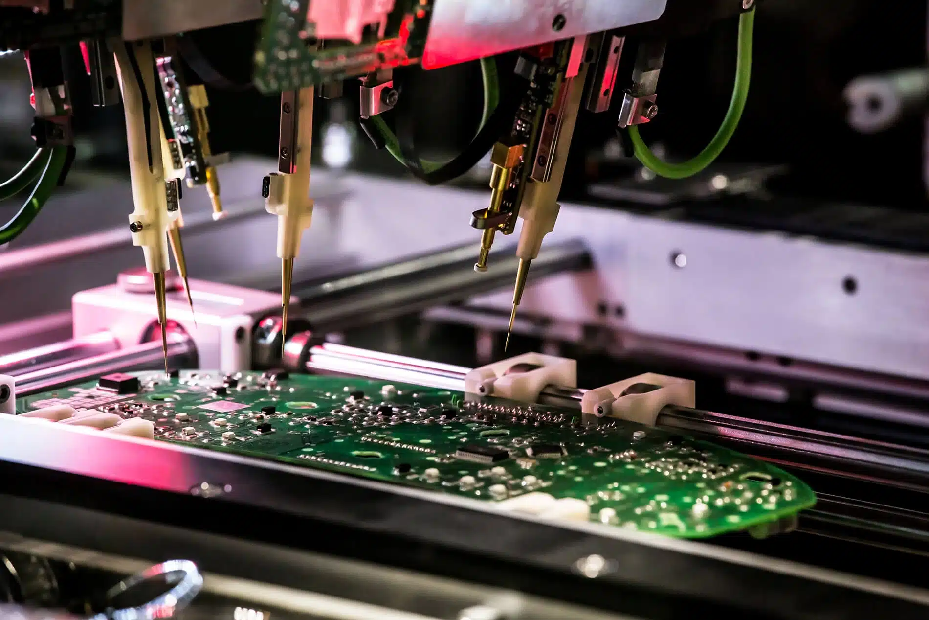
ICT tests the following:
- Dimensions of components, leads, and lands
- Markings on components
- Problems with soldering
- Shorts between traces and component leads
- Circuits with open connections (opens)
- Values of the resistors
- Passive components check
- Active components check
- Misoriented analog and digital components
- Values of capacitance and inductance
- Incorrect or missing components
Despite this, ICT cannot check multiple power connections, decoupling capacitors, mechanical fixings, and redundant power connections. Even though the testing method has its flaws, it remains one of the most effective ways to test a circuit board assembly.
Functional test
Performing functional testing on finished PCBs is the last step before approving the product. Functional testing is the most comprehensive way to determine if a manufactured board is ready for dispatch.
This test can identify the following signal problems:
- Power integrity issues – excessive ripple of power distribution network (PDN), low-frequency noise, and excessive jitter
- Various signal distortion issues, such as signal skew in buses and excessive distortion on several nets
- Due to incorrect component placement, a missing component, or excessive IR drop, the board might display incorrect voltage or current
Functional testing is not always accurate. There are many variabilities, including inputs, testing procedures, test plans, an outline of the desired results, and testing parameters. These variabilities make this testing method very complex.
Ensure error-free PCBA by following key design guidelines that prevent common assembly errors. Read our article, 6 design mistakes leading to PCB assembly errors, to know the common design errors that result in PCBA errors.
What should a PCB assembly inspection report include?
An inspection report should summarize all the necessary review values along with some key parameters that include:
- Reference designator: It is essential for identifying components. As a general rule, references are defined by a letter followed by a number. There will be a unique reference designator for each location on the PCB. For example, a resistor is denoted by “R” and a capacitor is indicated by “C”. However, there may be some variations in the letters, although they are standardized.
- Type of inspection test: This column defines the type of inspection test conducted on the given part. It includes AOI, X-ray, manual, ICT, and functional tests.
- Inspection result: (pass/fail)
- Defect found: Defects are marked in this column. It can range from stains, scratches to missing components.
- Action to repair PCB defects
- Remarks: These are specialized columns that categorize any crucial information or behavior related to the respective part. Additionally, it can be used to write non-conforming parts.
Board inspection quality requirements
To satisfy quality requirements, circuit boards should comply with specific standards. QMS (quality management system) calls for checking the vital points at each phase of the process to ensure the highest level of quality. Sierra Circuits is certified with ISO 9001:2015 standard. We check the quality at all the stages such as pre-production, production, pre-shipment inspection, and container loading supervision.
You can check all our certifications and registrations.
IPC A-610 standard contains all the quality assurance requirements for a populated board. The term quality refers to conforming to all the specifications standards and producing the necessary output. The QC process for board assembly involves testing, documenting, and validating the process. Compliance with these criteria accomplishes the quality requirements for an inspection report.
If you have any further questions about the PCB assembly inspection report, please let us know in the comments section. Check out our DFM design guide to learn about design for manufacturing aspects.

Design for Manufacturing Handbook
11 Chapters - 96 Pages - 90 Minute ReadWhat's Inside:
- Annular rings: avoid drill breakouts
- Vias: optimize your design
- Trace width and space: follow the best practices
- Solder mask and silkscreen: get the must-knows
Download Now