Contents

On-demand webinar
How Good is My Shield? An Introduction to Transfer Impedance and Shielding Effectiveness
by Karen Burnham
Most modern devices employ differential signaling to meet high-speed and high data-rate needs. Controlling differential signaling in rigid PCBs is simple if proper design principles and tools are used. However, handling differential signaling in flex circuits poses some design challenges.
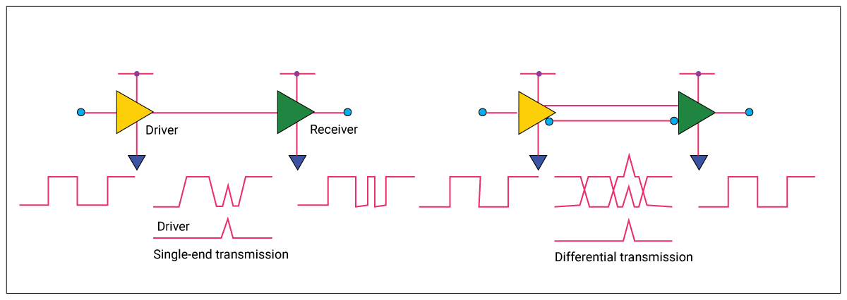
Two transmission lines with a common-mode signal on top of equal and opposing polarity signals form a differential pair. These two differential signals are equal and opposite and closely timed to one another. Apart from being equal, opposite, and closely timed, no other characteristics matter when a PCB design employs differential pairs.
Maintaining the equal and opposite amplitude and timing relationship are the prerequisites when using differential pairs. For example, a common-mode signal may be 1.5V with 0.25V differential signals riding on it. The line “A” of the differential pair could be (1.5V + 0.25V = 1.75V), and line “B” is (1.5V – 0.25V = 1.25V). The difference between the two lines is +0.5V. When the voltage on B (1.75V) is higher than the voltage on A (1.25V), the difference between A and B will be -0.5V. Because of the smaller difference in voltage between the two lines (which is only 0.5V here), differential pairs act faster than the single-ended line. Therefore, the signal speed on the differential traces is higher.
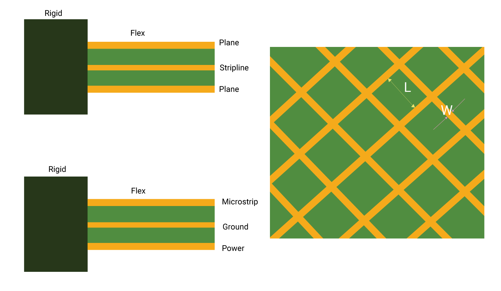
Differential signaling in flex circuits is achieved by designing them as a surface microstrip. This approach makes it possible to create high-speed, high-data-rate flex circuits. Differential signaling is used in these types of boards when employing HDMI, USB, and PCI Express.
When do you need differential signaling?
Differential signaling is required when:
- The ground connections between the ends of the signal path are weak
- There is a substantial attenuation along the signal path
- There is a requirement to send a lot of information in a short amount of time, i.e., high data rate needs
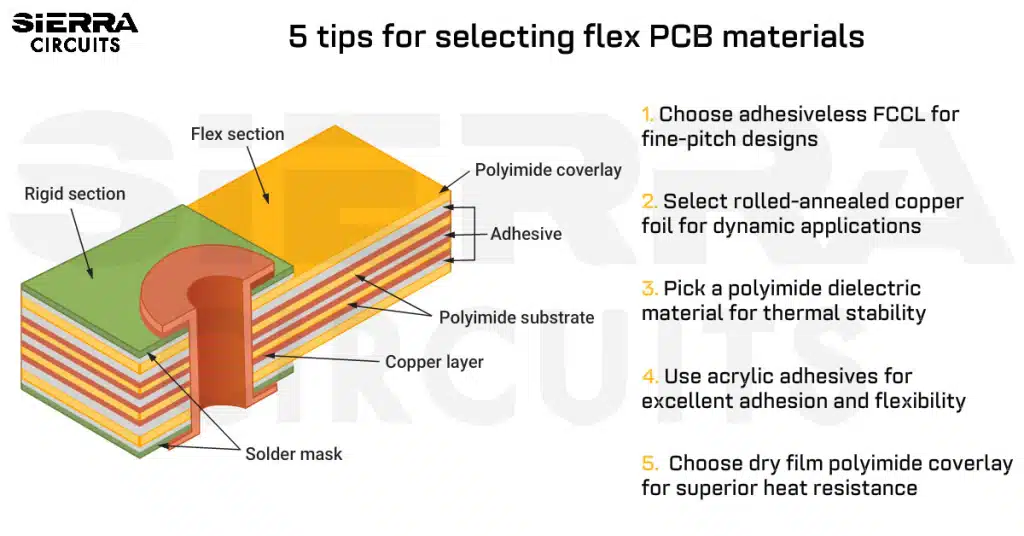
How to design flex boards to achieve differential signaling?
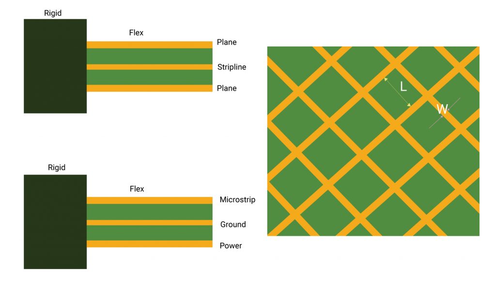
Differential signaling in flex circuit boards is the design method of surface microstrip transmission lines. Surface microstrip lines are formed by etching one surface of a double-sided material. The top surface and the sides of the traces are exposed to air and are referenced to a power or ground plane.
Microstrip allows for a thinner flexible PCB design (2 layers with a thin core), whereas stripline increases flex thickness considerably (3 layers with 2 thicker cores). A stripline PCB geometry is around 75% thicker than a microstrip design.
Shielding requirements are evaluated to determine which configuration will be suitable. In a nutshell, thinner controlled impedance trace widths support thinner copper and cores, resulting in improved flexibility and mechanical bend reliability.
To learn how to solve the reliability issues in rigid-flex designs, see the air gap construction method in rigid-flex PCBs.
Why differential pair for a digital or an analog signal path?
- The ground connection between the two ends of the signal path can be weak, hampering the data quality.
- The link can experience significant signal attenuation but, at the same time, can function as intended.
- Last but not least, differential pairs are used for data paths with very high data rates, such as gigabit and higher links. Differential paths can be derived at rates as high as 10Gb/s over copper tracks in standard PCB materials. On the other hand, the same cannot be done with single-ended lines.
To learn how to design transmission lines, download our e-book.

PCB Transmission Line eBook
5 Chapters - 20 Pages - 25 Minute ReadWhat's Inside:
- What is a PCB transmission line
- Signal speed and propagation delay
- Critical length, controlled impedance and rise/fall time
- Analyzing a PCB transmission line
Download Now
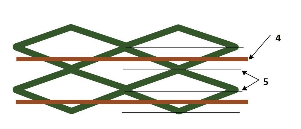
What is a cross-hatch or mesh ground plane in flexible PCBs?
Cross-hatching is a technique that makes specific planes or big regions of copper on a PCB seem like a copper lattice. Regular apertures are spaced at fixed intervals as shown in the image below. Cross hatching a plane is no longer required in rigid PCBs, but it is still utilized in flex and rigid-flex designs, where it can give numerous advantages.
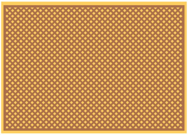
A cross-hatched plane is created in a CAD or CAM system. The hatched region is a filled area with a sequence of periodically spaced lines, similar to the traces plotted in signal layers. The region is then bordered by a thin trace that links the ends of the cross-hatched lines. Connections to this cross-hatching, such as power or ground connections, are established in the same way as they are in solid planes. The cross-hatch application in flexible PCBs is explained in the following sections.
- Impedance control in flex: A hatch ground is a useful way to provide the reference plane needed for controlled impedance routing on high-speed digital circuit boards. The hatch ground offers broader, more manufacturable dimensions while maintaining flexibility in both circuit and assembly. It’s worth noting that cross-hatching reduces the quantity of copper under a transmission line, lowers its capacitance, and increases the impedance.
- Providing structural support to the flex regions: The use of a hatch ground provides the structural support required for a dynamic or static flex ribbon without affecting the copper layer’s rigidity.
It is advised to use a modeling tool that accounts for the missing copper in the cross-hatched plane to determine the trace width needed for precise impedance. Since the impedance of a trace across the hatch ground zone is greater than that of the solid ground region, the inductance of the trace must be reduced to keep the impedance under control. This is the reason why a trace should be built a little wider. This lowers the inductance of the trace and raises the overall capacitance with respect to the hatch ground. Both techniques will adjust the impedance suitably.

Factors responsible for signal distortion in flex PCBs
Length of the interconnect
- The length of the PCB interconnection is directly proportional to signal distortion
- Compared to TEM (transverse electromagnetic mode) interconnects, the length of the board interconnects is essential in non-TEM interconnects that employ cross-hatching planes
Repetitive variation of dielectric constant due to cross-hatch
Cross-hatch introduces shunt resonances in flexible PCBs, lowering the signal amplitude to an undesirable level and reducing the effective usable bandwidth of the circuit board. It happens because of the periodic variation in the dielectric of the cross-hatch pattern and also because of the variation in copper length.
Misalignment of the signal traces in differential pairs
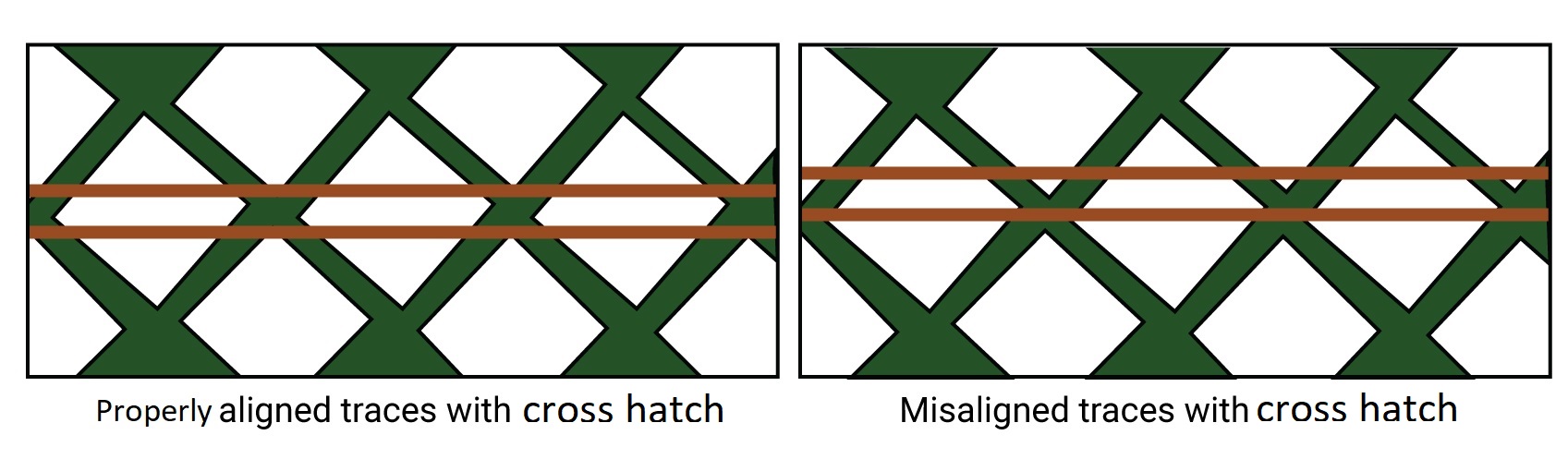
Misalignment of the signal traces and cross-hatched layers generates impedance asymmetries, and skew between the two signal traces in differential pair interconnects.
Crosstalk
The return currents associated with the two neighboring interconnects interfere when the return plane is cross-hatched, resulting in crosstalk. When one or more traces are sandwiched between two traces on the same layer for cross-hatched boards, crosstalk becomes a significant problem. This has the potential to reduce signal quality substantially.
Switching the cross-hatched pattern orientation from vertical to horizontal is the best way to minimize crosstalk.
Optimizing cross-hatch pattern to reduce signal distortion
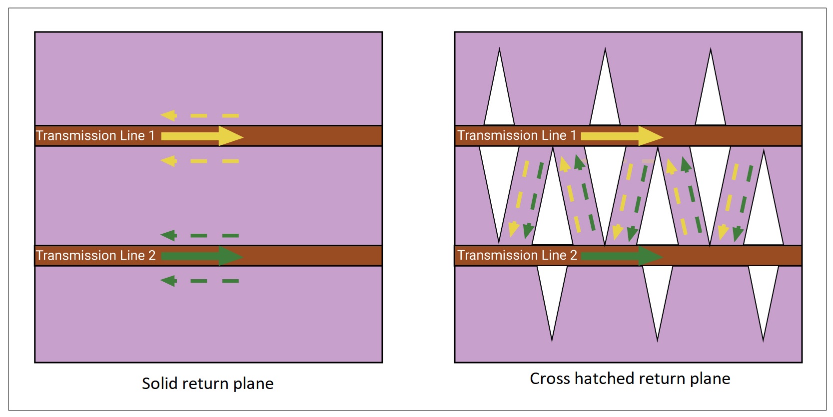
The return currents for each transmission line in the solid return plane flow in the opposite direction of the signal, ensuring that they do not interfere with one another. The currents traverse non-parallel return paths when the return plane is cross-hatched and when the electric and magnetic fields are not perpendicular (they are non-TEM). This results in signal distortion.
Although practically, it is not possible to make a cross-hatched return plane interconnect perform the same way a solid return plane does. Signal distortions can be reduced to acceptable levels by altering the size, shape, and orientation of the cross-hatched pattern in relation to the signal traces.
- Diamond-shaped cross-hatch patterns are preferred to square cross-hatched patterns. The longest length of the pattern should be parallel to the signal traces.
- The longest length of the cross-hatch pattern should be less than or equal to 1.27mm (50 mils).
- The shortest length of the cross-hatch pattern should be less than half of its longest.
4. Center-align the single-ended traces between cross-hatch intersections.
5. Implementing two or more cross-hatch intersections between each single-ended trace can reduce crosstalk.
6. Differential traces should straddle cross-hatch intersections.
7. Keeping one or more empty diamond-shaped cross hatches between differential pairs can minimize crosstalk.
8. Total transmission line length of less than 1 inch or 2.5cm causes less distortion than those with length more than 3 to 5 inches or 8 to 12cm.
Sierra Circuits manufactures and assembles the highest quality flex printed circuits. Visit flex and rigid-flex PCB capabilities to learn more.
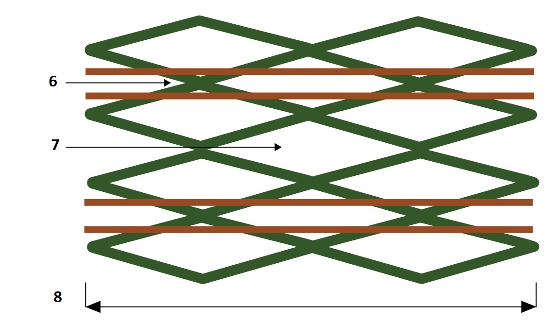
How to maintain signal integrity using a mesh ground plane in flexible PCBs?
In flex and rigid-flex boards, hatching or meshed ground plane is a popular approach for providing a constant 0V reference. This results in a big conductor that can shield across a wide frequency range while enabling the flex ribbon to bend and fold without becoming too rigid.
Hatching works the same way as any other ground plane does. Its purpose is to offer a constant reference for designing a trace with the required impedance. In rigid-flex or flex boards with a meshed ground plane, any of the standard transmission line geometries (microstrip, stripline, or waveguides) can be used. At low frequencies, a hatched copper zone on the flex ribbon’s surface layer produces almost the same effects as solid copper.
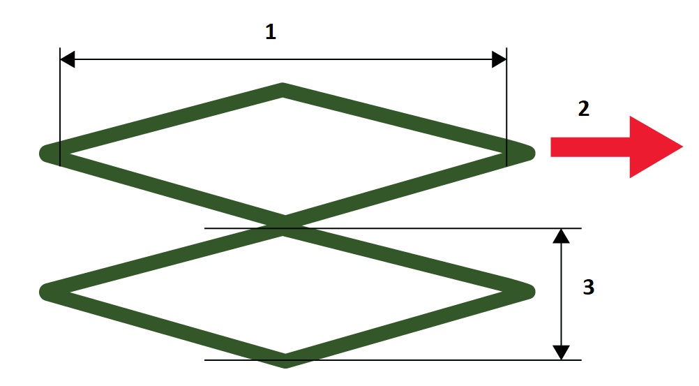
The common configuration for stripline and microstrip routing on a flex ribbon with mesh ground planes is shown below.
L and W are the two important geometric parameters of the mesh plane construction. These two variables may be combined to provide a fill factor or the percentage of the mesh area to be filled by copper. The following are the results of changing these parameters:
- Keeping all other parameters constant, increasing the mesh area (by increasing L) increases the impedance. It also makes bending the ribbon easier.
- When W is increased while keeping other parameters constant, the mesh area is closed, resulting in an increase in impedance. It makes bending the ribbon harder.
What are the advantages and disadvantages of differential signaling?
Advantages of differential signaling
- Common-mode noise in differential pairs is zero.
- Since they have a low return path across the grounding plane, signal reflections owing to ground return path error may be avoided.
- The signal-to-noise ratio (SNR) is improved by using differential pairs (SNR).
- Since the signals are routed closely, external noise reaches both of them at the same time and in the same amount. It increases the likelihood of noise rejection.
- Differential signals can be routed via noisy power boundaries and through analog/digital planes. This is one of the efficient methods to regulate EMI in the flex board.
Disadvantages of differential signaling
- Requires an appropriate routing method as well as careful consideration of length, space, and impedance
- Can cause problems and introduce a lot of noise if not routed precisely
Download this e-book to learn how to design a reliable flex PCB.
Flex PCB Design Guide
10 Chapters - 39 Pages - 45 Minute ReadWhat's Inside:
- Calculating the bend radius
- Annular ring and via specifications
- Build your flex stack-up
- Controlled impedance for flex
- The fab and drawing requirements
Download Now
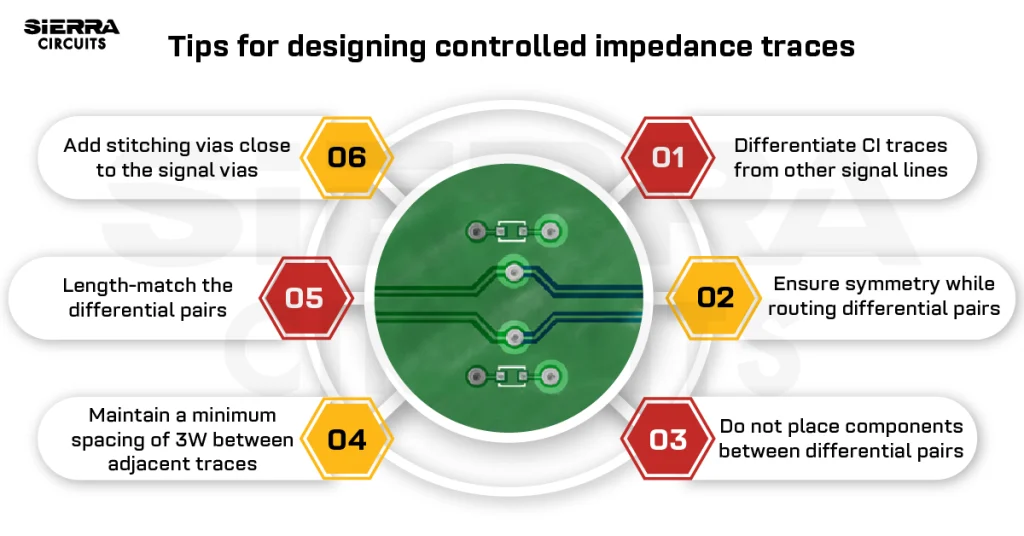
Tips for differential pair routing in flex PCBs
- Always match the length of the traces while routing a differential pair. The rise time at the receiver is used to establish the length-matching tolerance of a differential pair.
- Certain forms of differential signaling in flex require specific impedance matching in the PCB layout. In such instances, the width, spacing, and thickness of the routing must be matched.
- If one signal layer needs to be changed, then it’s a good idea to alter both signal layers at the same time. When the length of a via impacts signal balance, routing one signal on one layer and the other signal on another is a poor practice.
- A differential pair’s members do not have to be routed together.
- A “not closer than” criterion should be applied to members of a differential pair.
- The distance between the differential pair should be decided as per the stack-up design.
- Differential pairs with vias and right-angle bends are acceptable.
- AC coupling capacitors can be positioned anywhere throughout the differential pair’s length.
- It is okay to specify the single-ended impedance for each differential pair member.
- Differential pair parallel terminations should be sized on the high side of the PCB trace impedance tolerance.
- Since a PCB does not offer common mode noise reduction, crosstalk spacing regulations must account for this.
- PCB layout is more challenging with broadside differential pair routing than with coplanar routing.
- Reduce discontinuities by using a symmetrical approach. To ensure a clean launch, it may be necessary to forsake the 45-degree routing.
- Copper pour and stitching vias provide a safe environment for high-speed routing.
- The air gap between the lines is larger than the width of the lines themselves, indicating loose coupling. Certain discontinuities are acceptable with loose coupling. Tight coupling takes up less space and requires fewer bumps to accommodate corners in the routing.
Rules that are not applicable to differential signals routed on a PCB
- The return current for one member of a differential pair flows in the other member.
- Differential impedance is necessary for performing differential signaling.
- Signal integrity is improved with broadside differential pair routing.
Working with differential pairs is relatively more difficult than with single-ended connections. The difference is amplified in a flex circuit regime as it bends and has unusual angles. At the end of the day, we are just comparing two signals to check whether they’re in a HIGH or LOW logic state, and then moving on to the next one. Differential signaling in flex PCBs not only provides power saving but better noise cancellation as well.
Need assistance in designing differential pairs? Post your queries on the forum, SierraConnect. Our experts will resolve them.