
Contents
In this video, Keysight ADS SI application scientist Tim Wang Lee shows you how to use basic signal integrity (SI) analyses such as eye diagrams, S-parameters, TDR and single pulse response to solve signal integrity problems.
After learning the 3-step approach to solve signal integrity problems from the video, download the example to perform techniques widely used in the SI industry on your own.
Watch now and download the example files. Get a jumpstart on your own signal integrity analysis!
I’m Tim Wang Lee, an Application Engineer from Keysight Technologies, and this video is about how to solve signal integrity problems.
I will show you the three-step approach to solve signal integrity problems, talk about the essential Signal Integrity analyses, and apply the techniques to a case study!
Here are the three steps to solve signal integrity problems:
Number one, simulate the channel.
Number two, identify the root cause of degradation.
And number three, explore the design solutions.
To enable the three-step problem-solving process, we need a variety of signal integrity analysis techniques.
Throughout this video, I will be using an ADS (Advanced Design System) workspace.
The link to the workspace is available on the screen and also in the description.
To start solving signal integrity problems, we will first simulate the channel, given a channel, a transmitter and a receiver.
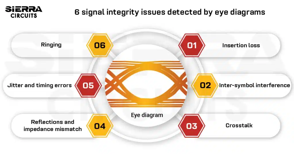
Eye Diagram Shows Channel Degradation
An eye diagram in PCB design tells us how much the channel degrades the transmitted signal.
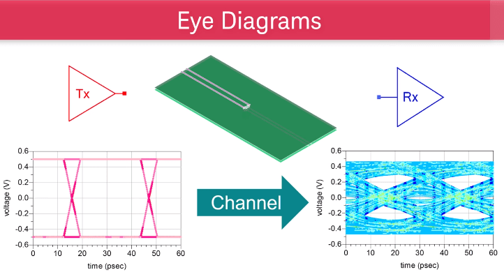
On the left, the eye at the transmitter side is open.
The digital 1 and 0 levels can be clearly distinguished.
However, after the signal goes through the channel and reaches the receiver, the eye is closed.
It will be hard for the receiver to tell a digital 1 from a 0, and we know we have a signal integrity problem.
To create an eye diagram, we start with a pseudorandom binary sequence (PRBS).
We then use our knowledge of Unit intervals (the UI’s) to slice the PRBS waveform.
We overlay the slices, so that all rising and falling edges can be seen.
Eye diagrams give us a concise graphical representation of how the channel degrades the signal.
Next, we will find the root cause of degradation with mixed-mode S-parameter analysis, and Time domain reflectometry.
If we have a section of transmission line, and send a sine wave of frequency F-naught at port 1, the S11 tells us how much of the sine wave is reflected back out of port 1.
It is the reflection coefficient and is related to the return loss.
The parameter S21 gives us information on how the transmission line transmits the sine wave.

Mixed-mode S-parameters Characterize the Differential Channel
It is the transmission coefficient and is related to the insertion loss.
When we are using a pair of transmission lines to transmit a differential signal from differential port 1, and differential port 2, mixed-mode S-parameters are used to tell us how the transmission lines react to differential and common signals.
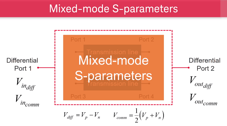
For example, SDD11 is a description of the differential response at port 1 excited by differential signal at port 1.
As the DD terms give you information about differential responses, CD terms show you how much common signal is generated by differential input signals.
DC terms show you how much differential signal is generated by common input signals.
As S-parameters tell us the frequency response of the channel, we will use time-domain reflectometry (TDR) for the spatial and timing information.
On this TDR impedance plot, the right-hand side is the open circuit to help us identify the end of the channel.
To create the TDR plot, we first express the channel impedance in terms of a known system reference impedance, Z-naught, and reflection coefficient, Gamma.
To find Gamma, we will need a step generator and a reflection monitor.
As the step generator produces an incident wave travelling down to the channel, the reflection monitor is capturing all the reflections.
By taking the ratio between incident wave and reflected wave, we can calculate Gamma.
And once Gamma is known, we can plot the impedance.
Finally, to explore design solutions, I will show you the single pulse response.
By sending a single pulse with specific rise time and data rate, we examine the single pulse response at the output.
Single Pulse Response Shows Inter-Symbol Interference (ISI)
Here is an example of a single pulse response.
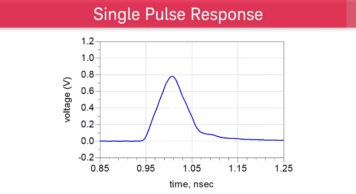
If we start with the maximum of the single pulse response and name it the cursor, we can create a cursor diagram by marking the single pulse response in terms of unit intervals.
The cursor diagram tells us how many pre-cursors and post-cursors the pulse response is spreading across.
We will see later that pre- and post- cursors are useful information for equalization.
The amount of spreading is also a good representation of inter-symbol interference.
Inter-symbol interference happens when current pulse leaks into adjacent pulses.
Now that we have the analysis tools, we will apply our approach to a case study: The Case of the Failing Channel.
I have designed a virtual channel with a differential pair that starts at the top microstrip layer, goes through a via transition, and ends up on a stripline layer.
Channel Simulation Example
Following the first step, we will simulate the channel.
After entering the needed information into the downloadable workspace, and simulating, I have all the analyses results.
From the Eye diagram analysis, we can see the transmitted signal, shown in red, is only outside of the eye mask and a digital 1 or 0 can be clearly distinguished.
However, when the signal reaches the receiver, there is an eye mask violation, and we have a signal integrity problem.
Knowing that we have a signal integrity problem, we will take the second step and identify the root cause of the degradation.
From the mixed-mode S-parameters, we notice that insertion loss has a dip at close to 20 GHz.
This dip might be degrading the eye.
To better understand this dip, let’s take a look at the channel again.
The first section is a 3 inch ~100 Ohm differential Microstrip line.
The second section is differential via transition.
The third section is a 3 inch ~100 Ohm differential stripline.
Since the first and third part are both transmission lines, we will group them together.
Given our data rate, (28 Gigabit per second) and the rule of thumb for channel attenuation, we expect the 6-inch line at the Nyquist frequency, 14 GHz, to have about 9 dB attenuation, which translates to -9 dB insertion loss, and there shouldn’t be any dips.

Transmission Line Model Confirms Expectation
Using transmission line models, we quickly confirm our expectation with simulation.
Looking at the eye diagram, with about 9 dB attenuation at 14 GHz, the eye is still open and almost passes the eye mask test.
The result of the investigation tells us that the transmission lines alone are not enough to cause the eye closure.
It is the via transition that’s degrading the performance of the channel.
To verify our theory, we will take a closer look at the via design, which is also included in the ADS workspace.
Follow the link to download.
In the via design, we see the via stubs when the traces transition from the microstrip layer to the stripline layer.
The stubs are about 75 mils.
Using the rule of thumb for quarter-wave length stub resonance in FR4, we expect a resonance at close to 20 GHz, close to the dip shown in the channel.
Simulating the via by itself, we confirm that the resonant frequency is consistent with the one in the mixed-mode S-parameter analysis.
To make sure there is a stub, we will do a consistency test in the time domain.
Because the via stub is in parallel with the feed on the stripline layer, transitioning from the via to the stripline layer feed, we should see a drop in the TDR impedance plot.

TDR Plot Shows Channel Impedance Profile
Let’s take a look at the TDR impedance plot.
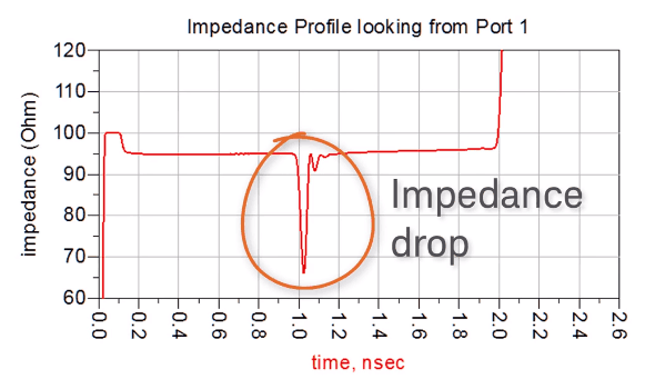
To make things clear, I placed the open circuit at the end of the stripline layer.
As expected, there is a large impedance drop in the TDR plot, confirming that there is a via stub.
At this point, we are sure of the root cause of our signal integrity problem.
The root cause is a via stub resonating at frequencies close to the Nyquist, resulting in a dip in the insertion loss, distorting the frequency spectrum of the input signal, and degrading the eye.
Having found the root cause of degradation to be the via stubs, we have arrived at the final step.
Explore design solutions.
Back-drilling is often done during the manufacturing process to remove the extra stub length and eliminate stub resonance.
Back-drilling can also be done in designs.
After removing the stubs, we expect the resonance to be gone, and the eye to open.
Sure enough, after I went back to my design and removed the stubs, the stub resonance is no longer there, and the eye opens.
In TDR, since there is no longer a stub in parallel with the feed in the stripline layer, the impedance plot doesn’t have the large low impedance drop anymore.
Although it is possible to remove stubs in manufacturing, the cost to back-drill can be high.
When the stubs cannot be removed, equalization can help open the eye.
Equalization to Optimize Channel Performance
In the time domain, decision feedback equalization uses digital signal processing to open the eye.
To explore the equalization solution, we will use the single pulse response, and the interactive cursor selection tool.
By using the interactive cursor selection tool, we can select the number of pre- or post- cursors we want to equalize.
We then toggle the write function to create a cursor definition file.
We will then apply equalization in a channel simulation.
Enabling Decision Feedback Equalization, and entering the cursor definitions files, we will open our closed eye.
From the simulation result, we can see that the eye was initially closed because of the via stub resonance.
After applying equalization, the eye opens.
In summary, we simulated the channel and saw the closed eye.
Using mixed-mode S-parameters and TDR, we identified and confirmed the root cause of degradation.
Finally, we looked at the single pulse response to select the number of pre- and post-cursors to include in our equalization setup.
Of course, there is a lot more detail about the analyses than I can cover here, but I’ve included it in an ADS workspace which you can download.
Get a head start on your signal integrity journey by using the workspace.
Thanks for watching!
Until next time, check your signal integrity often, and keep the eyes open.

Signal Integrity eBook
6 Chapters - 53 Pages - 60 Minute ReadWhat's Inside:
- Impedance discontinuities
- Crosstalk
- Reflections, ringing, overshoot and undershoot
- Via stubs
Download Now
About The Keysight ADS Team : Advanced Design System is the world’s leading electronic design automation software for RF, microwave, and high-speed digital applications. ADS pioneers the most innovative and powerful integrated circuit-3DEM-thermal simulation technologies used by leading companies in the wireless, high-speed networking, defense-aerospace, automotive and alternative energy industries. For 5G, IoT, multi-gigabit data link, radar, satellite and high-speed switched mode power supply designs, ADS provides an integrated simulation and verification environment to design high-performance hardware compliant with the latest wireless, high speed digital and military standards. Key Benefits of ADS Complete, integrated set of fast, accurate and easy-to-use 3D EM, circuit & system simulators Verification libraries for emerging wireless, automotive, and defense-aerospace standards Supported by leading IC foundry and industry partners