


Contents
Layout is the foundation of printed circuit board design. While initial blueprints are the starting point for designers, layout determines the reality and viability of PCBs. Not only does PCB layout involve the placement of components, it provides insight into how easily assembly and manufacturing can be accomplished.
Past entries in the Becoming a PCB Design Master series focused on assembly, quickturn, HDI and manufacturing. This entry will highlight the importance of PCB layout design, as well as some common mistakes all design masters should know to avoid.
To eliminate design errors, see how to perform pcb design review and layout clean-up.
Becoming a Layout Master
PCB layout can impact every element of circuit board design success. This makes it essential for designers to prioritize proper layout and incorporate best practices. The following tips will help designers do just that.
1. Select the Right Software
“Layout design software can cost thousands of dollars.”
There was a time when layout design had to be done manually. Today, there are numerous software solutions available to assist with PCB layout, making for faster, more efficient designs. However, as with every aspect of PCB design, choosing the right software requires careful thought.
Cost is often the primary obstacle. High-end layout design software can run in the thousands of dollars. In addition to cost, designers should focus on finding a software solution that will suit their specific needs, whether they’re corporate engineers, electronic hobbyists, or somewhere in between. It’s also vital to find software that is intuitive, as programs may feature complicated interfaces.
Finally, the software should feature a large library of components. Being forced to constantly create custom components increases the likelihood of errors.
2. Label for Future Reference
Modern software allows designers to use reference designators during PCB layout. However, these labels may not transfer over to physical circuit boards. It’s essential for designers to ensure labels used in layout are included on the final product.
Reference designators should not be placed under components. They should be situated close enough to their corresponding components to make sense for manufacturers. Additionally, the text used for these labels should be large enough to be easily identified. Users of electrical engineering and electronics community All About Circuits recommended fonts that are at minimum 0.060″ tall and 0.050″ wide.
Also read, mastering the art of PCB design basics.
3. Keep Space in Mind
As we highlighted in our Becoming a PCB Design Master article for HDI, space is at an all-time premium for PCBs due to demand for smaller devices.
Since smaller surface area means designers must utilize tinier components and place them closer together, choosing the proper layout technique is all the more important.

Using blind and buried vias is one way to maximize space. Meanwhile, designers may opt for smaller surface-mount packaging. While helpful, this can also lead to difficulties down the line, as smaller components and packages are inherently more difficult to place and maintain.
Designers must weigh their layout design against the needs of manufacturing to strike the right balance. The PCB design checklist helps them to build a high-quality board.
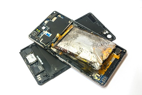
4. Account for Heat Issues
There are numerous details that require technical attention during the layout design process, from the proximity of traces to each other to ensuring the board has adequate airflow. However, one of the most important relates to heat dissipation. PCB layout should encourage optimal temperature levels at all times to ensure effective performance.
Materials used, the number of layers incorporated, and thermal path design will all impact the operating temperature of components. Using thermally conductive planes that spread heat evenly is one way to encourage greater heat dissipation. The use of heat sinks and thermal vias is also recommended.

Quote and order your circuit boards online with our SELF-SERVICE PCB tools in just a few minutes.
About Amit Bahl : Amit Bahl, widely recognized as the PCB Guy, earned his Bachelor of Science in Engineering from UCLA. He is currently the Chief Revenue Officer at Sierra Circuits, where he continues to lead efforts to simplify the PCB design journey and support designers and engineers in creating high-quality boards.


