



Contents

On-demand webinar
How Good is My Shield? An Introduction to Transfer Impedance and Shielding Effectiveness
by Karen Burnham
Medical PCB design mistakes, such as poor stack-up planning and inefficient thermal management, can lead to inaccurate readings, false warnings, and unexpected device behavior.
Understanding these common errors helps medtech circuit designers avoid performance issues and ensure accurate and stable device operation.
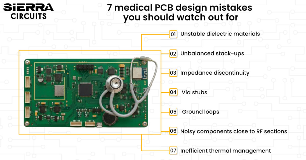
In this article, you’ll learn 7 medical circuit board design mistakes and solutions, the different types of boards used in healthcare devices, and the key industry standards for medtech PCBs.
Watch the full webinar here: Stop making these medtech PCB design mistakes.
Highlights:
- Select low-moisture, thermally stable laminates to withstand sterilization cycles and long-term operation.
- Implement symmetrical stack-ups with accurate impedance and dielectric details.
- Eliminate via stubs to reduce reflections in high-speed signal paths.
- Avoid split ground planes and weak stitching via structures that increase EMI and return path noise.
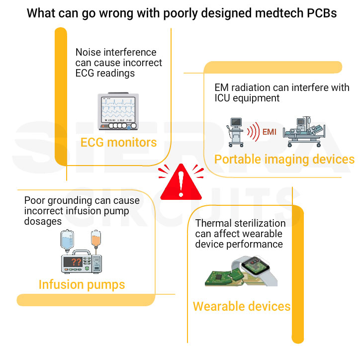
The infographic below explains the issues that can arise from poor medical PCB design practices.
1. Choosing laminates with unstable dielectric and thermal properties
Using substrates with an inconsistent dielectric constant increases signal loss. This becomes critical in MRI or ultrasound systems where signal clarity matters. Moisture absorption introduces instability in biosensor circuits.
The glass weave effect creates an uneven dielectric distribution. This results in skew and jitter in high-speed signals. CTE mismatch between copper and laminate creates mechanical stress. Over time, this can cause via cracking or delamination.
1.1 5 parameters you should consider when choosing medtech PCB materials
You should focus on five key characteristics: glass transition temperature (Tg), CTE, dielectric constant (Dk), dissipation factor (Df), and thermal conductivity (k). These properties directly influence signal quality.
| Material properties | Recommended value | Examples |
|---|---|---|
| Dielectric constant (Dk) | <4 | FR408HR (3.68), I-speed (3.64), and Tachyon-100G (3.02) |
| Dissipation factor (Df) | <0.005 | RO4350B (0.0037 at 10 GHz), I-Tera® MT40 (0.0031 at 10 GHz), and Megtron6 R-5775 (0.004 at 10 GHz) |
| Glass transition temperature (Tg) | >170°C | RO4003 C (280°C), Isola P95 (260°C), and Ventec VT-901 (250°C) |
| Coefficient of thermal expansion (CTE) | Close to copper (~17 ppm/°C in X/Y, <70 ppm/°C in Z-axis) | RO 4350B (32 ppm/°C in Z-axis), Panasonic Megtron 6 (45 ppm/°C in Z-axis), EM 390 (40 ppm/°C in Z-axis) |
| Thermal conductivity | >0.5 W/mK | Taconic TSM-DS3 (0.65 W/mK), RO3010 (0.95 W/mK), TC 600 (1.4 W/mK) |
2. Building unbalanced stack-ups with incomplete impedance definitions
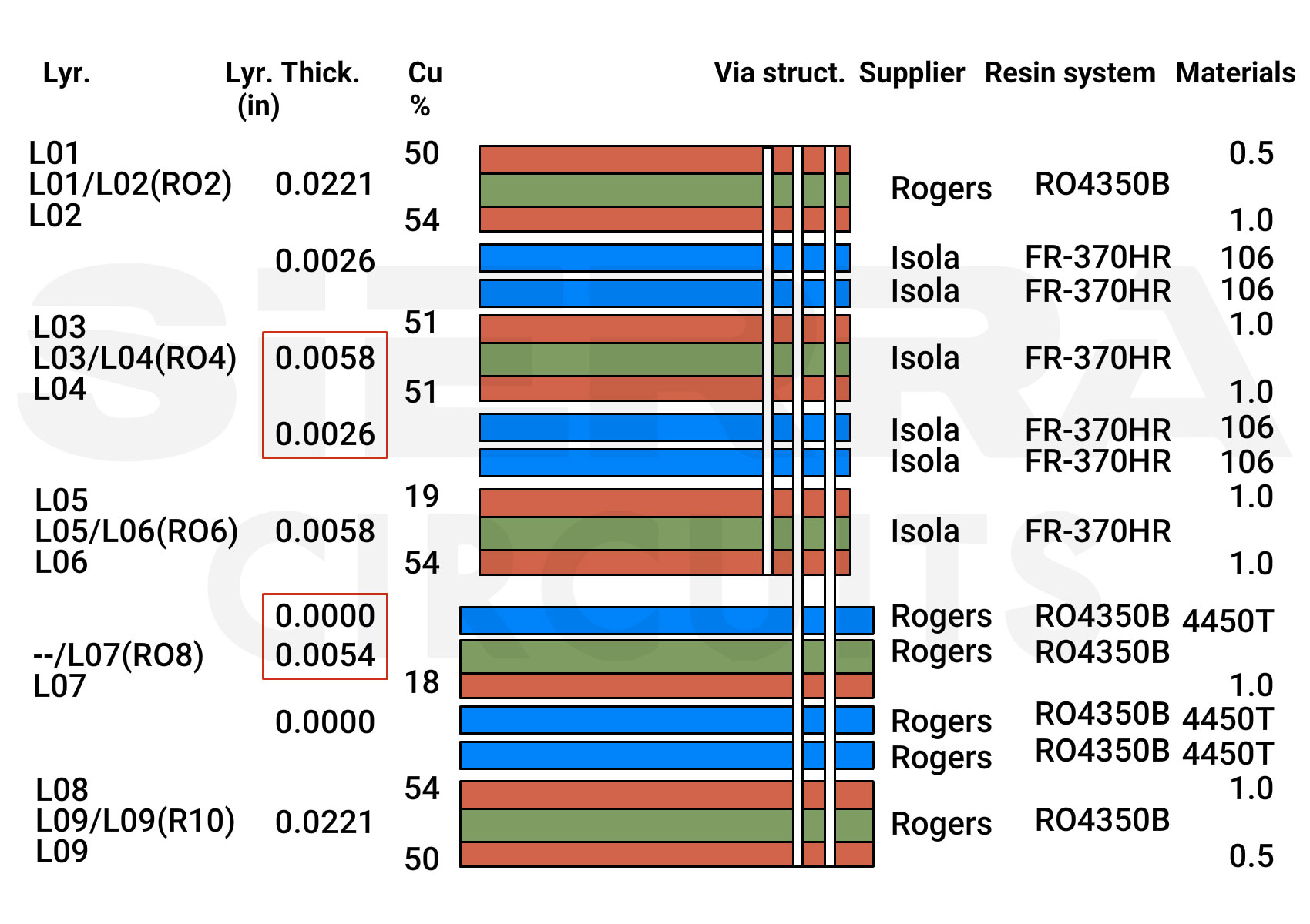
One of the most common medical PCB design mistakes is creating unbalanced stack-ups. It directly affects signal integrity.
Missing important impedance and material details in the stack-up also makes it difficult for the fabricator to understand the build-up requirements, often leading to unnecessary back-and-forth communication and fabrication delays.
Common stack-up mistakes are:
- Impedance defined without dielectric details
- Unbalanced stack-up construction
- Missing reference planes under signal layers
- Undefined or inconsistent copper weights
- Incorrect dielectric thickness used for impedance calculations
- Solder mask and surface finish not included in final thickness
These errors cause impedance variation and return path discontinuity. A clearly defined, symmetrical stack-up with complete material and impedance details ensures reliable manufacturing.
2.1 Best stack-up practices for healthcare PCBs
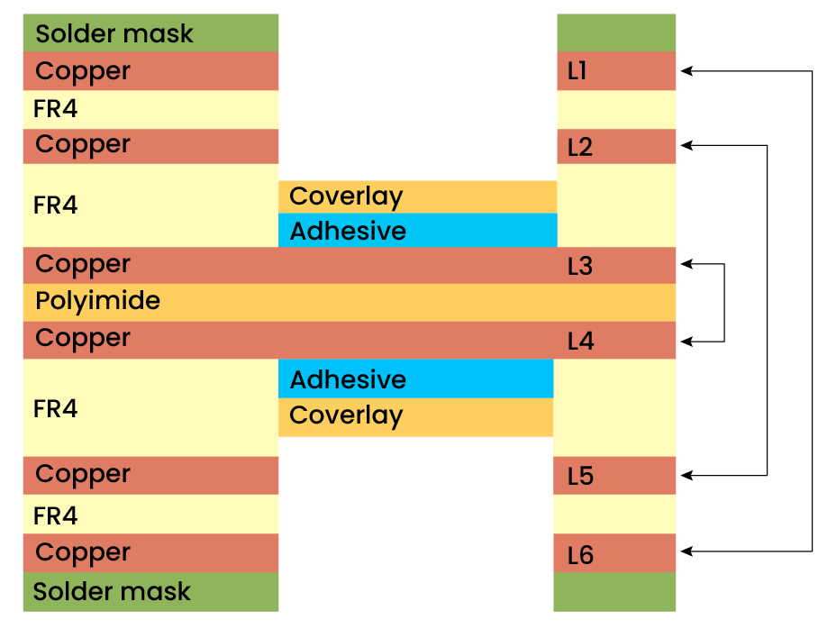
A well-balanced stack-up begins with symmetry. Copper weights and dielectric thickness should be mirrored across the board center. This helps to prevent bow and twist during fabrication and keeps the board mechanically stable.
To improve manufacturability, designers should:
- Define impedance values and tolerance (± 5–10%) in the stack-up data.
- Signal layers should be placed next to solid reference planes.
- Copper distribution across layers should remain balanced using pours or dummy fills.
- Specify dielectric materials and copper weights accurately.
- Define solder mask layers before the surface finish.
- Limit total lamination cycles (preferably, ≤4).
For more, download the PCB Stack-Up Design Guide.

PCB Stack-Up Design Guide
12 Chapters - 55 Pages - 60 Minute ReadWhat's Inside:
- Design guidelines for HDI, flex, and hybrid stack-ups
- Stack-up representation in fab drawing
- DFM checks for layer stacks
- Characteristics of high-speed materials
- Manufacturing tolerances
- PCB stack-up examples with illustrations
Download Now
3. Breaking impedance continuity in critical signal paths
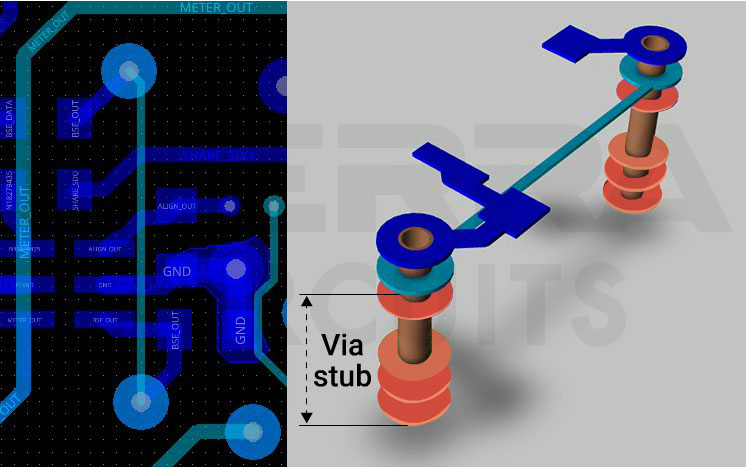
Impedance discontinuities often appear at signal transitions. They typically occur at:
- Connector interface
- Unused stubs or long pads that behave like resonators
- Sudden trace width or spacing variations
- Undesired splits, or gaps in reference planes
If these discontinuities are not addressed, they introduce signal reflections and degrade signal quality in sensitive medical electronics.

3.1 How to maintain uniform impedance in medical PCB layouts
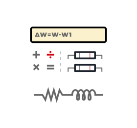
Uniform impedance can be achieved by keeping trace widths and spacing consistent, using gradual tapers during width transitions, and matching track impedance with connectors and antenna feedlines.
The following techniques help to stabilize impedance and improve overall signal performance:
- Maintain uniform line widths.
- Gradually taper traces when dimensions change.
- Maintain 3W to 5W spacing between traces to minimize crosstalk.
- Ensure the trace impedance matches the connector impedance.
- Taper traces to match the connector pin width. E.g, adjust the microstrip line (50 Ω) width to match the SMA pin dimension.

Taper down the traces to minimize signal degradation. - Use LC matching networks, such as π, T, or L networks, in antenna feedlines.
- Implement λ/4 transformers when transitioning between components and antenna feedlines.
- Provide solder mask openings over critical RF traces.
4. Ignoring via stub effects and poor layer transitions
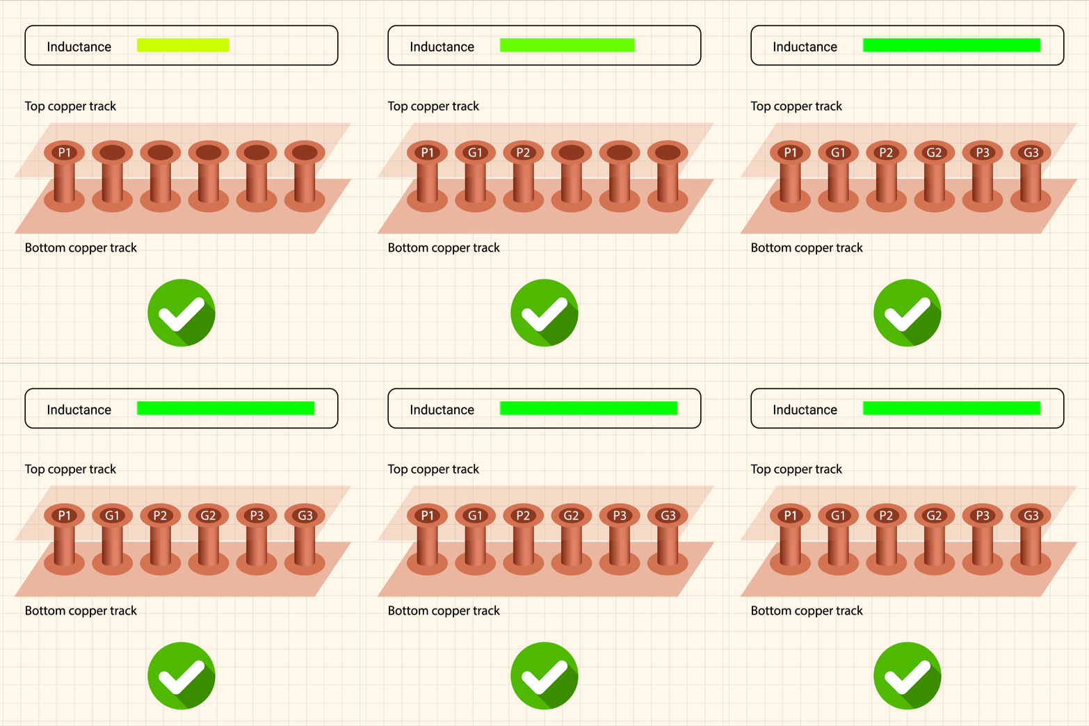
Layer transitions should be carefully designed in dense medical PCB layouts, especially in high-speed and RF designs. Every via introduces a discontinuity in the signal path. If hole geometry and stub length are not controlled, they can create reflections, parasitic inductance, and resonance effects that degrade measurement accuracy in healthcare devices.
4.1 Via design practices for reducing reflections and parasitic effects
- Place vias as close as possible to minimize inductance.
- Reduce via diameters to 8 – 16 mil to avoid parasitic effects.
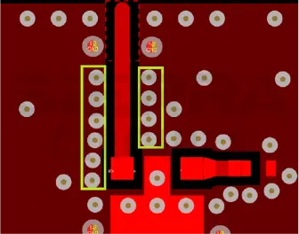
- Position vias evenly along both sides of transmission lines to isolate noise from adjacent traces.
- Avoid placing power and signal vias next to each other.
- Insert ground vias between power and signal vias to reduce loop area.
- Ensure via impedance matches the impedance of the connecting RF trace.
- Keep the via stub length within 1/20 wavelength of the resonant frequency.
- Use blind or buried microvias to eliminate stubs.
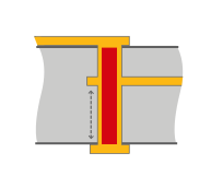
You can also use back drilling to remove via stubs. However, this approach requires careful consideration. The sudden change in via barrel geometry can introduce localized impedance discontinuities and reflections. Use back drilling only when it becomes necessary.
5. Creating noisy ground loops and split return planes
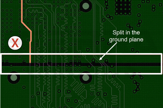
Ground loops and split planes can introduce noise, increase electromagnetic interference, and reduce signal accuracy. These issues often appear unintentionally during layout when return current paths are not designed efficiently.
Other common grounding mistakes include:
- Routing RF signals over gaps or slots in ground planes.
- Inadequate stitching vias between layers, which leads to high impedance return paths.
- Polygons or Isolated ground pads not tied to ground planes.
- Metal enclosures, shields, or cans not connected to ground planes.
- Using thin traces instead of solid copper ground pours.
- Sharing RF ground with noisy switching circuits, such as switching power supplies or microcontrollers.
To learn how to mitigate electromagnetic interference, download EMI and EMC Design Guidelines for PCBs.
EMI and EMC Design Guidelines for PCBs
6 Chapters - 77 Pages - 75 Minute ReadWhat's Inside:
- How electromagnetic interference is generated and spreads
- How to identify EMC requirements and applicable standards
- How to design for electromagnetic resilience
- Common EMI sources: Switching circuits, PWM signals, and motors
- PCB structures that cause radiated emissions
- Practical layout, stack-up, filtering, and shielding guidelines
Download Now
5.1 Grounding and stitching strategies for low-noise medtech PCB layouts
A well-designed grounding structure helps maintain stable return current paths, reduce EMI, and improve signal integrity in sensitive analog and RF circuits.
Follow these best grounding and stitching via practices:
- Avoid splits/slots in ground planes.
- Ensure a solid ground plane under ICs for return current flow.
- Fill spaces between shield cavities and circuits with ground copper pours.
- Use solid ground fills instead of hatched patterns.
- Make sure the copper pour is grounded correctly. A floating ground pour might resonate like an antenna.
- Maintain spacing between trace and ground pour around 1.5 to 2 times the trace width.
- Keep stitching via spacing between λ/20 and λ/10 of the signal’s operating wavelength.
5 grounding myths that cause medical PCB failures
| Myth | Reality |
|---|---|
| Splitting ground planes reduces interference | Splits force return currents to detour, increasing loop area, EMI, and signal distortion |
| Any ground via is good enough | Poor via placement and sparse stitching vias create high inductance paths |
| The chassis and ground plane can be tied anywhere | An incorrect chassis-to-ground plane connection creates long return loops and radiated emissions |
| More copper pour = better grounding | Isolated large copper pours might act as antennas |
| Low-frequency rules apply to high-speed designs | At high frequencies, return currents follow the path of least impedance, not least resistance; this misunderstanding often leads to EMI issues |
6. Placing noisy components close to sensitive analog and RF sections
Poor part placement can introduce interference, increase parasitic effects, and reduce measurement accuracy in sensitive analog and RF circuits. These sections should be isolated from noisy digital circuits such as switching regulators, microcontrollers, and high-speed interfaces to prevent noise coupling.
6.1 Component placement strategies for healthcare PCB layouts
- Place decoupling capacitors close to IC power pins.
- Maintain spacing between RF sections and switching circuits.
- Position antennas away from metal components, heatsinks, ground planes, and other conductors to prevent detuning.
- Maintain clear and linear signal flow paths.
- Reduce unnecessary trace length to minimize parasitic effects.
- Position sensitive components, such as antennas, at the board corners to minimize interference from other elements.
For more on antenna placement, see antenna integration and RF design guidelines for 5G PCBs.
7. Neglecting thermal planning in compact medical devices
High-power ICs such as processors, FPGAs, and PMICs generate significant heat due to switching activity and current density.
Common heat sources in medtech PCBs are:
- High-power ICs such as processors, FPGAs, and PMICs
- Voltage regulators and DC-DC converters
- Temperature-sensitive analog circuits
- LEDs and imaging modules
- Charging circuits and battery management systems
Need help in designing your medical PCBs? Our engineering team can help you with stack-up design, grounding strategies, and DFM analysis.
You can book a meeting with our experts or call us at +1 (800) 763-7503.

7.1 Heat dissipation techniques for medtech PCBs
- Avoid routing signal traces or vias beneath thermal pads. This might lead to coupling.
- Use at least 4 spokes around thermal relief pads for balanced heat dissipation. The spoke width should be 1/3rd to 1/2 of the pad diameter.
- Apply thermal interface materials (TIMs) between hotspots and heat sinks.
- Include thermal vias directly under the thermal pads for circuit boards with more than 0.7 mm (28 mil) thickness.
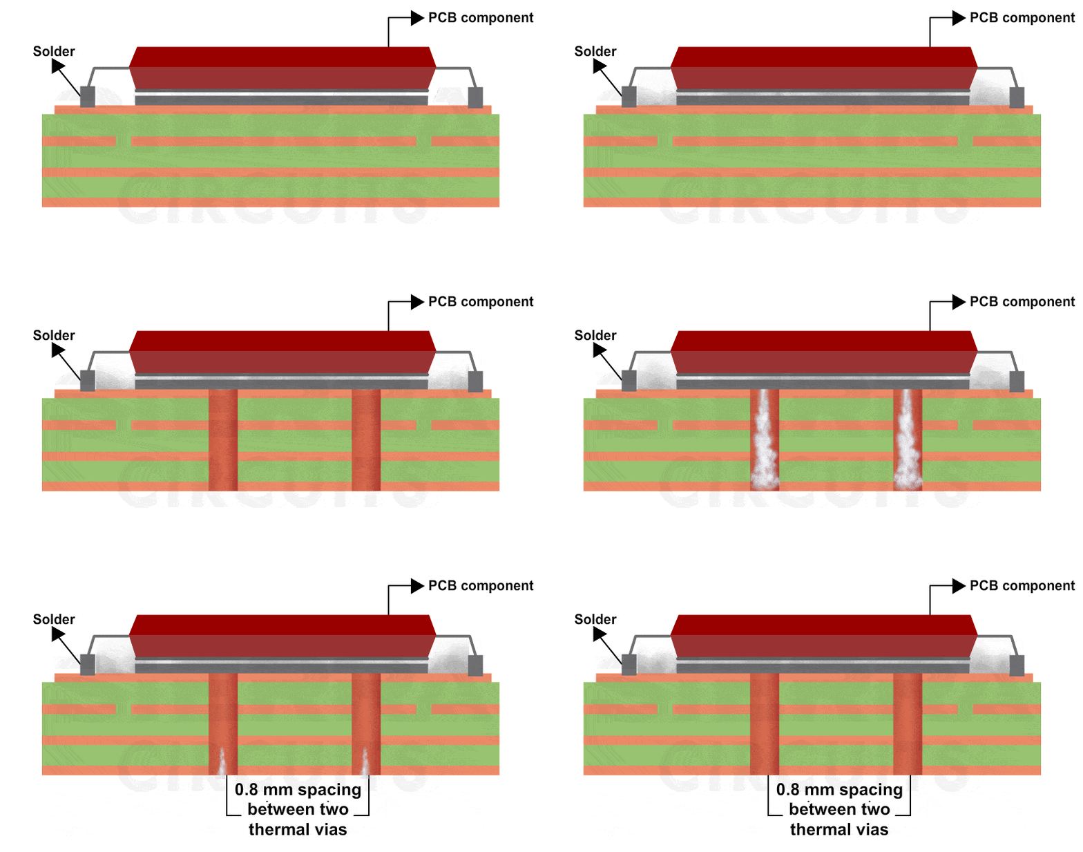
Position thermal vias close to heat-generating components to ensure efficient heat dissipation in medical PCBs. - Connect the heat sink to copper planes or thermal vias
- Use a via diameter of 0.3 mm (12 mil) and a via-to-via distance of 0.8 mm (31 mil).
Types of PCBs used in medical devices
The table below summarizes common PCB types and their typical medical applications.
| Type of PCB | PCB | Application |
|---|---|---|
| Rigid | 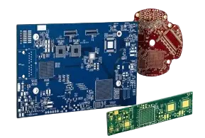 |
Patient monitors, ultrasound systems, and MRI control boards |
| Flex | 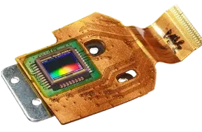 |
Wearable ECG patches, hearing aids, and implantable devices |
| Rigid-flex | 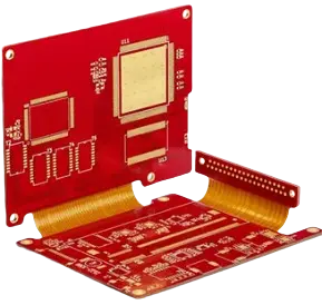 |
Surgical tools, endoscopy systems, portable diagnostic devices |
| RF/Microwave | 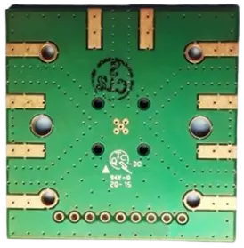 |
Wireless patient monitoring, telemetry modules, MRI systems |
Sierra Circuits manufactures high-quality rigid-flex circuit boards. Check the capabilities for more details.
Why are medtech PCBs different from standard electronics?
Medical devices work with extremely small signals compared to consumer electronics. Even a small noise or a small change in impedance can impact measurement accuracy. This makes layout decisions far more critical.
These devices must also operate consistently for long periods. During that time, they experience sterilization cycles, humidity, temperature changes, and mechanical stress.
Standards such as IEC 60601 and ISO 13485 require traceability and documented design decisions. Every layout choice must support safety and reliability. Because of these constraints, selecting the right PCB technology becomes the first critical decision.
To learn about key traceability elements for medical boards, see what is traceability in PCB manufaturing?
Industry standards for designing medtech PCBs
| Standard | Scope | Why it matters in PCB design |
|---|---|---|
| IEC 60601-1 | General safety for medical electrical equipment | Defines isolation, creepage/clearance, and protection requirements that directly impact PCB layout |
| IEC 60601-1-2 | EMC requirements for medical devices | Drives shielding, grounding, filtering, and layout practices to pass EMI/EMC tests |
| ISO 13485 | Quality management systems for medical devices | Ensures accurate design documentation, traceability, and process consistency |
| ISO 14971 | Risk management for medical devices | Requires identifying and mitigating risks. Influences layout decisions for safety-critical circuits |
| IPC-2221/IPC-2222 | General PCB design standards | Provides guidelines for layout, spacing, and reliability |
| IPC-6012 class 3 | High-reliability PCB fabrication | Ensures stricter fabrication requirements for critical medical applications |
| IPC-A-600/IPC-A-610 | PCB acceptability and assembly standards | Defines quality criteria for manufacturing and assembly |
| UL 94 | Flammability of PCB materials | Ensures materials meet fire safety requirements |
| RoHS/REACH | Environmental compliance | Restricts hazardous substances in materials used in PCBs |
For more, see medtech PCB design considerations with IPC and UL standards.
Medical PCB design mistakes often begin with small layout and material decisions, but their impact can be significant in healthcare applications. Issues such as unstable laminates and impedance discontinuities can lead to EMI problems and signal degradation.
By understanding and avoiding these errors, engineers can improve signal integrity, reduce manufacturing risks, and ensure stable operation in critical healthcare devices.
About the technical reviewer:
Abhishek Chari is the Team Lead for PCB Design at Sierra Circuits, with 6 years of experience specializing in high-speed PCB layouts and advanced HDI technologies. He possesses deep expertise in leading EDA tools, including Altium Designer, Cadence Allegro, Eagle PCB, and KiCAD.
Need help in designing your medtech PCBs? Post your queries on our forum, and our experts will answer them.











Start the discussion at sierraconnect.protoexpress.com