Contents
One of the primary prerequisites for manufacturing a reliable circuit board is having a high-quality soldering process.
IPC-J-STD-001 and IPC-A-610 define the acceptance criteria for electrical connectivity and materials used. The updates made to these standards are termed the H revisions of soldering standards.
As a designer, it is crucial to know the industry standards and their revisions to ensure a high-quality board. IPC revises these benchmarks once every three years to make the products suit the developing technology.
In this article, you will learn about the new H-revisions in soldering standards, followed by your CM for assembling your PCBs.
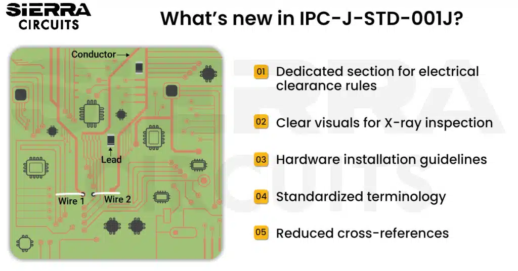
Highlights:
- IPC-A-610 focuses on visual inspection and acceptability criteria.
- IPC-J-STD-001 defines detailed soldering process, material, and equipment requirements for PCB assemblies.
- The H revision of J-STD-001 introduced key updates, including circumferential solder separation, insulation clearance, toe overhang limits, and thermal plane soldering criteria.
What is the difference between IPC-A-610 and J-STD-001?
IPC-A-610 and J-STD-001 both define specifications for PCB assembly and acceptance criteria for class 1, class 2, and class 3 boards.
However, J-STD-001 additionally includes detailed requirements for materials, equipment, and soldering processes, while IPC-A-610 focuses primarily on acceptability and inspection standards.
H revisions of the soldering standard J-STD-001 were released in September 2020. These new criteria modify the specifications related to maximum component overhang, circumferential solder separation, thermal protection, insulation sleeving, thermal plane, wrapped terminals, cleaning, and residue requirements.
The table below summarizes the differences between these two documents:
| Parameters | IPC-A-610 | J-STD-001 |
|---|---|---|
| Component placement and footprint alignment | Present | Present |
| Material requirements | Absent | Present |
| Common soldering issues | Present | Present but limited |
| Spacing requirements | Present | Present |
| Inspection criteria | Present | Present |
| Cleaning standards | Present | Present |
| Equipment requirements | Absent | Present |
For DFM tips, download the Design for Manufacturing Handbook.

Design for Manufacturing Handbook
11 Chapters - 96 Pages - 90 Minute ReadWhat's Inside:
- Annular rings: avoid drill breakouts
- Vias: optimize your design
- Trace width and space: follow the best practices
- Solder mask and silkscreen: get the must-knows
Download Now
What is the current revision of J-STD-001?
The current version of IPC J-STD-001 is revision IPC-JSTD-001J, released in March 2024.
The earlier H revision, published in September 2020, introduced several important updates, including editorial improvements, typo corrections, technical changes, and new acceptance criteria.
Here are some significant changes made to the document.
- Homonyms have been made clear because words like “lead” have two different meanings. A lead can be a component termination feature, and it can also refer to a metal alloy.
- To avoid confusion in the document, the new revision instructs you to use the symbol “Pb” if the word refers to the metal alloy. For instance, a lead should be referred to as Pb, lead-free as Pb-free.
To know more about circuit board acceptability standards, see IPC 6012 or IPC-A-600 which standard should you use?
7 technical revisions of IPC-J-STD-001
1. Paragraph 1
The information related to magnetic windings, high-frequency, and high voltage is moved to 1.5.3 as specialized technology. There are no significant changes in the content. However, a different section is created.
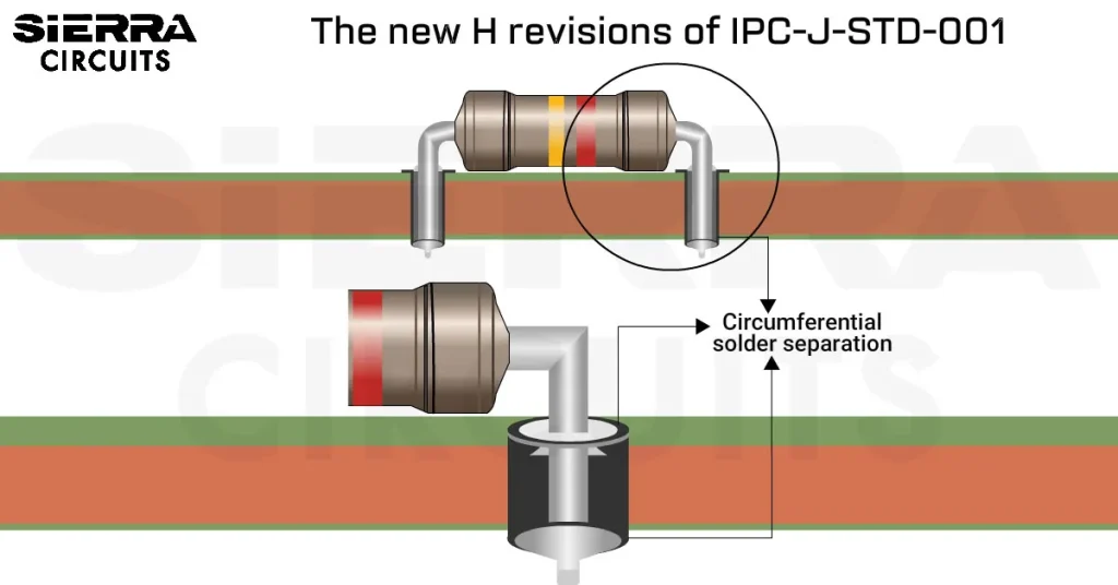
A new term, named circumferential solder separation, is added in section 1.8.1.

The word refers to an internal gap in the solder fillet that surrounds the complete diameter of a plated through-hole lead or wire. There is no solder fillet in the hole because there is no continuous solder from the source and destination side fillets. An X-ray inspection of a through-hole connection will show this. This is because when you add solder to a hole’s sides, it seems to be a void from a cross-sectional view.
The new soldering standards made it clear in 1.10.1 that a certified person is not necessary to conduct a non-destructive examination.
2. Paragraph 3
The process requirements that are added to paragraph 3 are taken from other sections of the document. It covers the soldering specifications for the materials, components, and equipment.
3.2.1 states that class 2 and 3 manufacturing processes must include a documented method that reduces the risk of cross-contamination between Pb and Pb-free products. This requirement is in addition to the standards for solder paste.
3. Paragraph 4
Another significant criterion is added in 4.4, which elaborates on improving thermal management.
According to this section:
- You must replace the heat-sensitive components that come into contact with the soldering heat source, such as an iron tip or other manual soldering tool.
- Adopt the safety measures while placing components or when you make manual assembly adjustments, like jumper wires.
Two more sections have been added in the H revision of the soldering standard. 4.17 adds threaded fastener criteria for process verification of J-STD-001, and 4.18 defines the torque requirements.
4. Paragraph 5
In 5.4.1.4, a statement of wiring overlap is added. Any wire that crosses over with itself or other wires is acceptable for class 1, but is considered defective for class 2 and 3 boards. Also, if it is wrapped in the opposite direction, it is acceptable for class 1 and class 2, and a defect for class 3. This condition can be exempted if the wire or lead is supported to prevent stress on the solder connection.
5.4.1.5 is renamed as insulation sleeving, which defines the insulation clearance. The standards are as follows:
- When the terminal opening is > 1 wire dia (1WD) to the base, then the insulation clearance shall be < 2 wire dia (2WD) and the insulation must cover the solder connection.
- When the terminal opening is < 1 wire dia (1WD) to the base, then the insulation clearance shall be < 1 wire dia (1WD)
To learn how to build reliable class 3 boards, download the IPC Class 3 Design Guide.

IPC Class 3 Design Guide
8 Chapters - 23 Pages - 35 Minute ReadWhat's Inside:
- IPC guidelines for manufacturing defects
- IPC standards for assembly processes
- Common differences between the classes
- IPC documents to set the level of acceptance criteria
Download Now
5. Paragraph 7
There are some notable changes in the surface mount components, which are covered in paragraph 7.
These changes include:
- A criterion has been added in 7.5.4 for rectangular chip (square-side termination) components.

Square-sided component. - In 7.5.7 flat gull-wing leads, some recommendations are added.
- Minimum heat fillet height is no longer based on the lead thickness.
- Maximum toe overhang is based on lead length.
- If the lead length is greater than or equal to 3 times its width, toe overhang is permitted.
- If the lead length is lesser than 3 times its width, toe overhang is not permitted for classes 2 and 3.

- Flat lug leads (power dissipating solid leads) and flat unformed leads are separated and added in two different sections for clarity.
- Standards for soldering requirements of the thermal plane in 7.5.15 are updated as follows:
When the manufacturer and the customer have not specified the criteria, the solder connection shall be larger than 50% of the thermal pad wetting area for classes 2 and 3. - Another modification to the bottom termination components (BTC) criteria is that the customer has to specify the minimum toe fillet height.
- 7.5.16, which is the bottom thermal plane connection, states that end overhang is allowed when all other criteria have been met because an end overhang is not a failure mechanism, whereas it is considered a solder anomaly.

- A new section 7.5.19 is added as a criterion with vertical cylindrical cans with outwards L-shaped lead terminations.

6. Paragraph 8
This paragraph gives complete details on cleaning and residue requirements. The specifications for an efficient soldering process are listed in 8.1. This includes:
- The cleaning procedure should be documented. You should also record the levels of soldering flux and other residues after the process.
- The hardware must not be harmed during the cleaning process. You need to document and provide objective evidence.
- If any rework procedures are done, you must include the qualifying document.
Section 8.2 addresses ionic process monitoring, and the subparagraphs include the requirements of:
- Sampling inspection plan (8.2.1)
- Control limits (8.2.2 )
- Exceeding the control limits (8.2.3)
7. Addition of Appendix D
Appendix D is a compilation of applicable through-hole X-ray criteria, and it does not specify any soldering requirements.
According to the first paragraph, you need to provide information about the use of X-rays to check through-hole solder conditions that are unavailable by any other method.
Sierra Circuits employs advanced technologies and software to fabricate and assemble your board as per IPC-610-A and J-STD-001 guidelines.
Visit our PCB manufacturing capabilities to learn more.
What are the major updates made to IPC-A-610?
Some of the important revisions incorporated in the document are:
- The target condition is removed throughout the document. You can set the standards as per your requirements.
- As mentioned in IPC-STD-J-001, clarity on the usage of the word lead and lead-free is explained here.
Technical edits of IPC-A-610
The following definitions are added in paragraph 1:
- Common conductor: Electrical conductors with the same current frequency, polarity, or potential.
- Strand diameter: Outside diameter of an individual metal filament used in a stranded wire.
- Form, fit, and function: Distinguishing feature, if not met, would adversely impact the assembly and cause failure.
- Non-common conductor: Conductors that carry different charges or frequencies.
- Kink: A tight or abrupt bend in a wire or component lead that clearly lowers the diameter or thickness of the conductor and cannot be eliminated by straightening.
Other changes in the document include:
- Sections 4.4 and 4.5 are taken from the IPC-A-610. These sections demonstrated how to secure wire bundles and how to route wires and bundles, respectively.
- Cooling lines and secondary reflow have been updated as separate sections in the H revisions.
- Heat-shrinkable soldering devices with the criteria from IPC-A-620 have been added to IPC-A-610. These devices are heat shrink tubing with a solder preform in the center of the device and can have sealing rings at each end of the tube. These devices are used for quick splices of wires or leads.
- A new soldering anomaly has been added in the form of solder inclusions. Any object that penetrates or projects out of the solder fillet is considered a defect.
- Criteria are added in 7.2.2.2 for adhesive bonding of elevated components that are taller. This is not a new section; however, the revision has given clarification on adhesive bonding for components such as box capacitors.
- There are modifications in section 8.3.5; the criteria for maximum toe overhang have been split, and the allowed overhang is now based on the length of the lead foot. The minimum heel fillet height does not depend on lead thickness.

- In paragraph 8.3.13, it is stated that the thermal plane can have up to 50% voiding if there are no specifications by the customer.

- Another addition is in 8.3.19 on wrapped terminals. It is the same as IPC-J-STD001H.
- Definitions for encapsulated and entrapped have been added in the subparagraphs of paragraph 10.
- In accordance with other IPC standards, section 10.8.3 is updated with a table that includes the coating thickness.
- The criteria for the solderless wrap are removed.
The new H revisions of soldering standards bring out some important content reorganizations and technical modifications in the document. They provide clear information on significant factors like flat gull-wing leads, toe overhang, insulation clearance, cleaning, and residue requirements.
Need assistance in designing your PCBs? Post your queries on our forum, SierraConnect, and our experts will answer them.