


Contents
The IPC-J-STD-001J revision, released in March 2024, groups electrical clearance rules into a dedicated section, improves inspection guidance through clearer acceptance criteria, and enhances X-ray interpretation with better visuals for identifying solder joint defects.
Awareness of these updates helps PCB designers in understanding quality expectations during layout development. It also streamlines communications between the manufacturing, assembly, and inspection teams.
In this article, you’ll learn about the key updates in the IPC-J-STD-001J version and how it can help engineers with their workflow.
Highlights:
- J revision of the soldering standard provides clear hardware installation guidelines, helping designers account for mechanical constraints early in the layout stage.
- It aligns design, assembly, and inspection expectations, reducing miscommunication and improving manufacturing efficiency.
- The update enables designers to minimize rework by making requirements easier to interpret and apply during layout development.
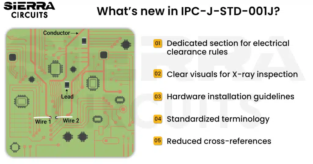
5 major updates in the IPC-J-STD-001J revision
This version introduces several improvements that focus on simplifying navigation, reducing confusion, and helping engineers work more efficiently across design, assembly, and inspection aspects.
1. Dedicated section for electrical clearance requirements
Earlier versions scattered clearance guidelines across multiple sections, forcing engineers to spend more time locating the required rules and slowing down the process.
The updated version consolidates all spacing rules into a single, dedicated section. This makes the document much easier to use in practical situations. Engineers no longer have to search through several pages to locate the right information, making design decisions and DFM analysis easier.
To learn how to get your boards easily manufactured, download the Design for Manufacturing Handbook.

Design for Manufacturing Handbook
11 Chapters - 96 Pages - 90 Minute ReadWhat's Inside:
- Annular rings: avoid drill breakouts
- Vias: optimize your design
- Trace width and space: follow the best practices
- Solder mask and silkscreen: get the must-knows
Download Now
2. Clear visuals for interpreting X-ray inspection results
Modern PCB assemblies often have solder joints that are hidden and cannot be checked with the naked eye. In such situations, X-ray inspection becomes extremely important.

The new updates in IPC-J-STD-001 improve the inspection process by adding more visual examples that help inspectors identify defects such as voids, bubbles, and incomplete solder joints.
Designers working with fine-pitch BGAs, QFNs, and other advanced SMDs can better understand quality expectations for hidden solder joints, enabling them to create inspection-friendly component layouts.
3. New hardware installation guidelines
The J revision provides clear guidance for installing mechanical hardware used during PCB assembly. This includes:
- Screws: Used to secure PCBs to enclosures or chassis.
- Nuts and bolts: Implemented for fastening structural components.
- Washers: Help distribute pressure and protect the board surface.
- Standoffs and spacers: Incorporated to maintain proper spacing between the PCB and the enclosure.

Earlier versions focused on soldering processes with limited clarity on hardware installation.
This helps designers to account for mechanical constraints early, preventing stress on solder joints and improving long-term reliability, especially in medical, aerospace, and defense applications.
4. Standardized terminology across the document
Technical explanations can sometimes be confusing, especially when similar words are used in different situations. For instance, terms like lead can create confusion, as a component lead may be misinterpreted as lead (the metallic element used in soldering).

To make things clear, new updates in IPC-J-STD-001 revision now explain the meaning of commonly used terms, such as:
- Wire: It is a single insulated electrical conductor used to connect points within a circuit or form external connections like harnesses or jumpers on a PCB.
- Lead: In electronic components such as resistors, capacitors, or ICs, the lead is the metal part that connects the component to the circuit. It is positioned on the PCB and soldered in place, creating a secure electrical connection with the circuit.
- Conductor: It is a material through which electricity can flow easily. In PCB design, it usually refers to copper elements like traces, pads, vias, and planes that create electrical paths on the board.

5. Reduced cross-references
IPC-J-STD-001H version included cross-references and similar guidance across multiple sections.
For example, guidelines on solder joint acceptability or cleanliness requirements may require engineers to refer to multiple sections due to cross-references.
The J revision reduces this need by removing repeated references, making the standard easier to navigate.
For engineers who regularly work with IPC soldering standards, this clearer structure reduces the need to jump between sections and makes it faster to locate the required information.
Download the IPC Standards Handbook for more details.
IPC Standards Handbook
7 Chapters - 110 Pages - 85 Minute ReadWhat's Inside:
- Clear breakdown of IPC standards for every stage of PCB development
- Design and DFM guidelines based on IPC-2221, IPC-7351, and IPC-J-STD-001
- Material selection guidance tied to IPC-4101, IPC-4202, and more
- Testing and inspection insights using IPC-A-600 and IPC-TM-650
- Best design documentation practices for seamless production
Download Now
IPC-J-STD-001H vs. IPC-J-STD-001J revisions
The table below shows the key differences between IPC-J-STD-001H and J revisions of the soldering standard.
| Updates | IPC-J-STD-OOIH | IPC-J-STD-OOIJ |
|---|---|---|
| Focus of the revision | Provide technical updates to soldering processes | Improve clarity, inspection guidance, and document structure |
| Electrical clearance requirements | Mentioned across multiple sections | Consolidated into one section for easier reference |
| Hardware installation | Limited guidance | New guidelines included |
| Inspection support | Basic inspection guidance | Improved X-ray inspection visuals with examples |
| Terminology | Defined with limited standardization | Standardized definitions (wire, lead, and conductor) |
At Sierra Circuits, we follow a structured approach to stay aligned with the latest IPC standard revisions. Our engineering and quality teams evaluate each update to identify its impact on assembly, inspection, and documentation practices.
For the IPC-J-STD-001J revision, we focused on key areas such as:
- Internal soldering process documentation
- Inspection guidelines and quality control procedures
- Training materials for operators and inspectors
To talk to a PCB expert: Book a meeting or call us at +1 (800) 763-7503.
How IPC-J-STD-001J helps PCB designers reduce errors
The new update minimizes design flaws by making soldering and inspection requirements easier to locate, interpret, and apply during layout development.
Earlier revisions required engineers to navigate multiple sections and interpret requirements that were not clearly structured. The J update addresses this by organizing the guidelines, improving terminology, and clarifying inspection expectations.
This helps designers:
- Avoid misinterpretation of requirements: Clear definitions and structured guidelines reduce guesswork during layout and documentation.
- Verify constraints faster during design: Consolidated sections, such as electrical clearance rules, make it easier to check the benchmarks without cross-referencing multiple parts of the standard.
- Design with inspection in mind: Improved X-ray guidance helps engineers account for hidden solder joints in BGAs, QFNs, and similar electronic components.
- Reduce back-and-forth communication with manufacturing teams: Better alignment between design, assembly, and inspection minimizes clarification cycles.
- Minimize redesigns/reworks: Fewer interpretation errors during layout lead to fewer issues during assembly and inspection.
Design mistakes that impact the solder quality of your PCB
| Design mistake | What can go wrong | How to avoid it |
|---|---|---|
| Improper pad geometry | Insufficient/excess solder, poor wetting, bridging | Use IPC-recommended land patterns |
| Incorrect use of SMD vs NSMD pads | Poor wetting, inconsistent fillets, weak joints | Prefer NSMD for better wetting and use SMD where mechanical strength is required |
| Unfilled via-in-pad | Solder wicking, voiding | Use filled and capped vias; avoid via-in-pad unless necessary |
| Insufficient component spacing | Bridging, shadowing, and rework difficulty | Maintain spacing for inspection, cleaning, and rework access |
| Inadequate solder mask clearance | Mask encroachment or excessive exposure | Define proper mask expansion and account for fabrication tolerances |
| Uneven copper distribution | Tombstoning | Balance copper, use proper thermal reliefs |
| Incorrect surface finish selection | Oxidation, poor solderability | Use ENIG/ENEPIG and ensure proper storage and handling |
All these mistakes lead to assembly defects, and your board may fail the quality checks defined in IPC-J-STD-001J. Avoiding them early in the design stage ensures higher yield, reduces rework, and helps your board pass inspection the first time.
Sierra Circuits fabricates and assembles high-quality circuit boards in the United States. With advanced DFA insights and rigorous testing, we deliver reliable boards.
To learn more, see PCB assembly capabilities.
Role of IPC-A-610J in PCB assembly inspection
IPC-A-610J defines how to check and evaluate completed assemblies, whereas IPC-J-STD-001J defines how to perform soldering.

In March 2024, the IPC released the IPC-A-610J standard along with the J revision of IPC-J-STD-001. These updates help inspectors interpret solder joint conditions more consistently during quality checks.
Need assistance in designing your board? Post your queries on our forum, SierraConnect, and our PCB experts will answer them.


Start the discussion at sierraconnect.protoexpress.com