Contents

On-demand webinar
How Good is My Shield? An Introduction to Transfer Impedance and Shielding Effectiveness
by Karen Burnham
Happy Holden is the authoritative leader on High-Density Interconnect. Anytime we talk to Happy, we always come back with new information for our customers. He has shared Tips for Designing HDI PCBs on our blog and was mentioned in our article discussing the History of HDI. When we talked last, Happy not only answered all of my HDI questions, but he also included a few tips for PCB designers working with HDI. Continue reading to find out the top three things to consider when getting into HDI design.
Top 5 things to consider when getting into HDI PCB
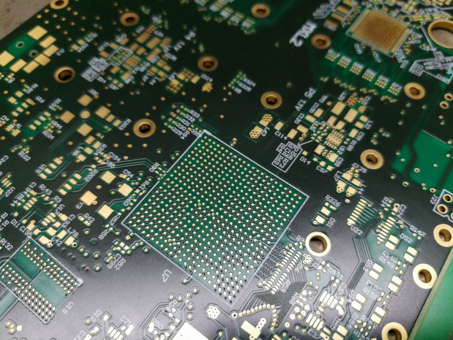
Stack-up architecture
In conventional multilayer boards, your design choices depend on the number of signal layers you require. HDI offers a larger variety of design choices. Choose from blind and buried, sequential buildup, or stacked and staggered, as well as many other design choices. Of course, HDI doesn’t require complex architectures. One of the most common mistakes designers make is creating architectures that are unnecessarily complex.
HDI materials
Pay attention to the materials used in your HDI design. HDI materials are covered by IPC 4104, but multilayers are covered by IPC 4101. IPC 4104 is an entirely different group of materials. Working with IPC 4101 brings about an entirely new set of constraints and rules that designers will need to familiarize themselves with.
HDI testability: How to ensure success on your first HDI design
As a designer, the testability of your board should always be taken into consideration. When you use blind and buried layers and you begin eliminating through-holes, testability is even more crucial.
I advocate that the first HDI board you should ever design should be a test vehicle, where you test the material and guarantee testability. Then you can do testing on reliability for the whole thing before you actually design your product. Your first HDI design can be successful, but there is also the possibility it will be painful and costly. If you can begin with a test vehicle, keep these things in mind: work with your fabricator, understand their testability guarantee, what the reliability is, and the material’s overall performance. This will aid you in the profit and performance of your future design.
Before designing begins, figure out if you require HDI
HDI designs require upfront planning. I often see designs where laser drills and blind vias have been added at the last step. This is typical because people don’t necessarily want to design HDI. They’re designing a finer chip or they’re putting more parts together, and they get the board 80% – 90% completed and they are via starved. They’ve run out of places for vias. The only way to finish the design is to add hundreds of laser-drilled blind vias. That will certainly work, but that is the worst-case scenario in terms of cost. You’re paying for HDI but you’re not benefiting from any of HDI’s advantages. HDI really requires that you plan for HDI design far before you start to turn on the CAD system. In other words, what are my design rules? What are my materials? What is the wiring density?
The thing I like to tell people is that an optimized HDI board can cost less than a through-hole board, and offer more reliability and higher electrical performance. But it doesn’t happen by accident. It takes a lot of skill and experience. We hear, “I don’t use HDI because it costs too much.” It only costs too much because the designer has to learn how to take advantage of HDI. It can cost less or be the same, but it depends on the designer’s education.
Learn How to Master HDI PCB Design
Controlled impedance
Controlled impedance is its own issue. HDI has thinner dielectrics than traditional boards, so if you’re looking for a traditional 50 Ohm single-ended or 100 Ohm differential pair, the thinner dielectrics will require smaller traces. That’s why it’s called high-density. You can design with 5 mil trace and space, but it’s a lot better if you’re using 3.5 mil trace and space, as that matches the 3 or 4 mil dielectrics on the build-up. As such, it’s important that the fabricator know how to control the tolerance of a 3.5 or 3 mil trace, in order to meet that characteristic impedance.

It’s fortunate Sierra understands how to build substrates. The highest technology in the PCB world is IC substrates. Since they supply prototype substrates with 25 micron lines and spaces, they understand high density. Those things are typically not controlled impedance, because they’re under the critical length of a transmission line. However, the substrate uses up the entire critical length. When you buy the package, everything you do must be transmission lines because the package has used up that critical length on the right side. So it’s not just fine lines, it’s the tolerance of those fine lines that are really important.

HDI PCB Design Guide
5 Chapters - 52 Pages - 60 Minute ReadWhat's Inside:
- Planning your stack-up and microvia structure
- Choosing the right materials
- Signal integrity and controlled impedance in HDI
- Manufacturing considerations for higher yields
Download Now
Check out Happy Holden’s The HDI Handbook.
About Amit Bahl : Amit Bahl, widely recognized as the PCB Guy, earned his Bachelor of Science in Engineering from UCLA. He is currently the Chief Revenue Officer at Sierra Circuits, where he continues to lead efforts to simplify the PCB design journey and support designers and engineers in creating high-quality boards.