Contents

On-demand webinar
How Good is My Shield? An Introduction to Transfer Impedance and Shielding Effectiveness
by Karen Burnham
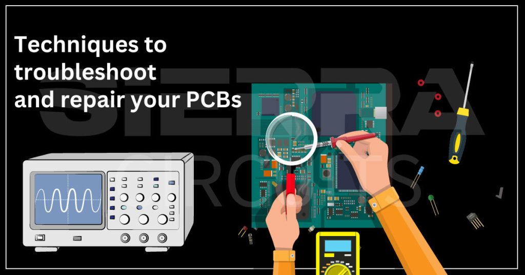
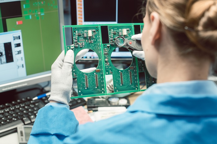
By troubleshooting and repairing a PCB, you will extend the lifespan of the circuit, which is both cost-efficient and time-saving. This process may seem like a difficult task, particularly for designs with complex layouts. However, you can easily identify the issue and mitigate it by following the sequential steps discussed in this article.
Remember, your circuit board has stood the test of time. It has endured all types of deterioration, like harsh weather, corrosion, and physical damage. If it has failed or malfunctioned, restoring it can be difficult. So, depending on its condition, decide whether you want to repair it or replace it before starting the restoration process.
You can also encounter faulty circuit boards after the assembly process. Depending on the nature of the defect, you can repair and recover the board.
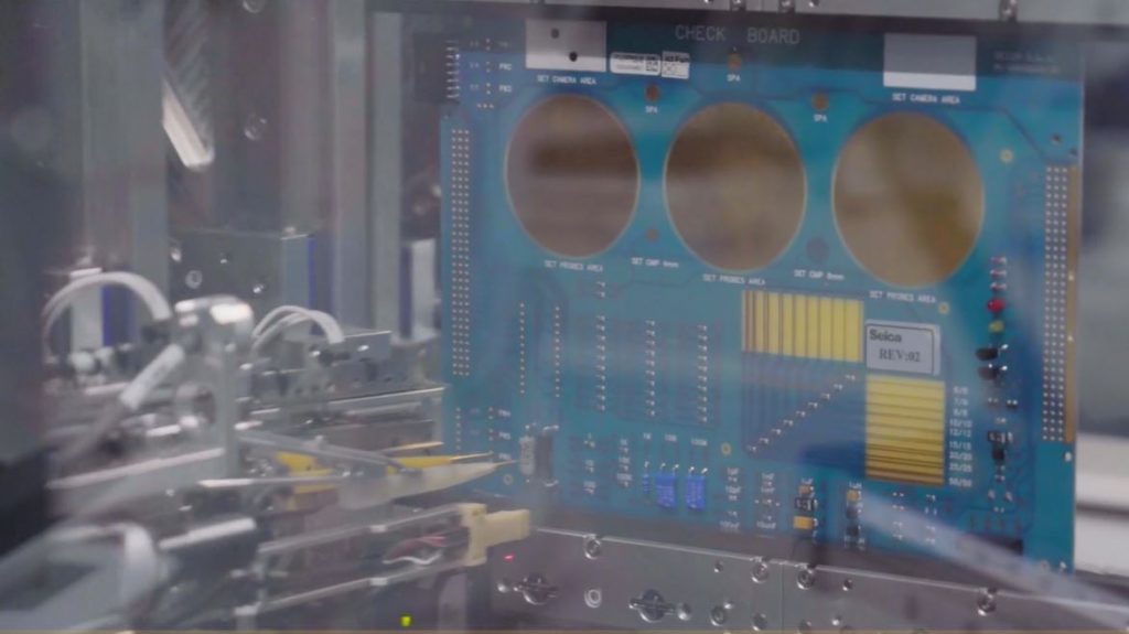
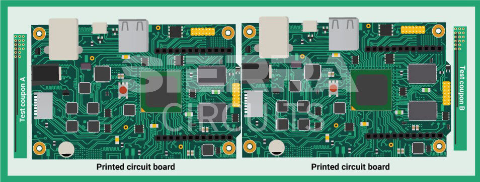
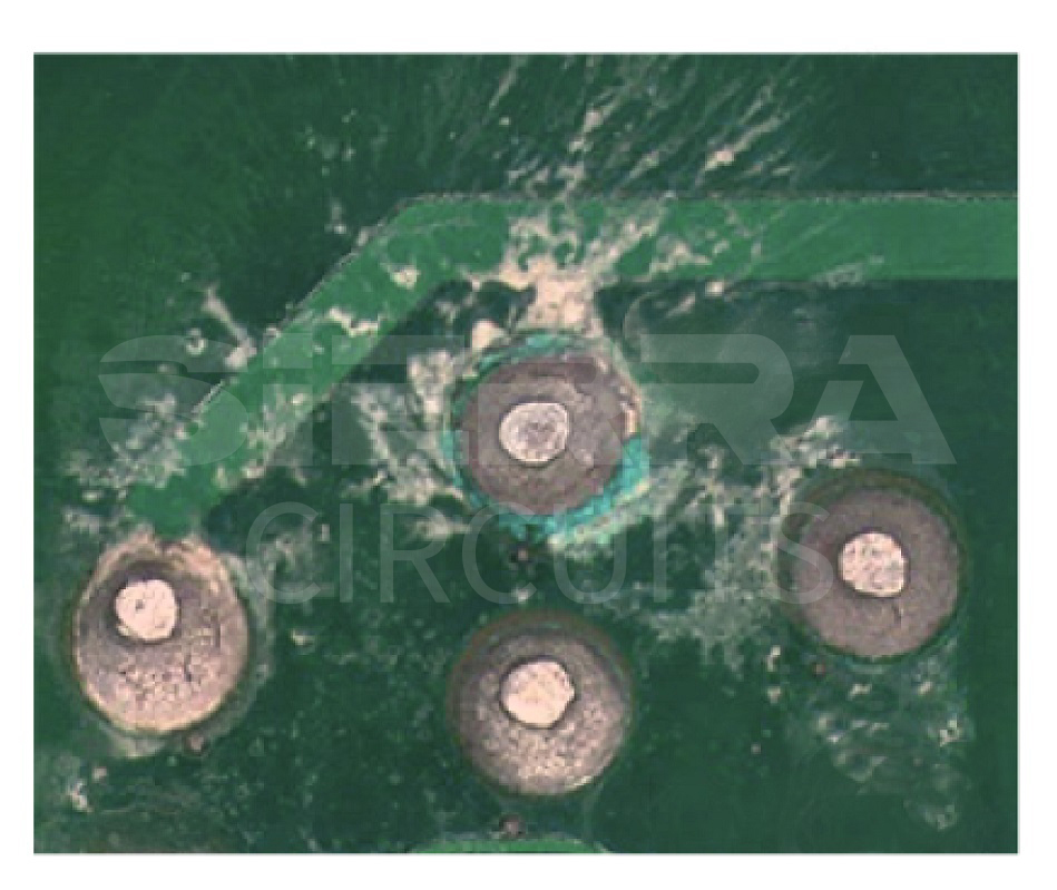
Quality control in PCB manufacturing
Based on the processes, the availability of equipment in the fab house, and the knowledge of the technician, you can opt for the following methods:
Using an automatic optical inspection machine
The AOI machine automatically scans for any missing components, improper solder (tilt or tombstone), and other defects on the board. Here, the device captures multiple images of the board using a camera and compares them to a reference board. When it finds mismatches, it indicates them as possible errors. Later, the technician analyses and rectifies the issue.
Flying probe testing for all nets
The flying probe test will assist you in identifying shorts, open circuits, incorrect parts (diodes and transistors), and defects in the IC’s diode protection. Short circuits and component faults can be rectified by using various PCB repair methods. However, if you encounter an open circuit, it can be challenging to resolve the issue, especially in HDI circuit boards.
To learn more about common board assembly defects, see the Design for Assembly Handbook.

PCB Design for Assembly Handbook
6 Chapters - 50 Pages - 70 Minute ReadWhat's Inside:
- Recommended layout for components
- Common PCB assembly defects
- Factors that impact the cost of the PCB assembly, including:
- Component packages
- Board assembly volumes
Download Now
Typical causes of PCB damage
Understanding the reason for the board failure can help you isolate the errors. Here are a few common causes:
- Components malfunction/breakdown: Replacing the defective part can help restore the original circuit.
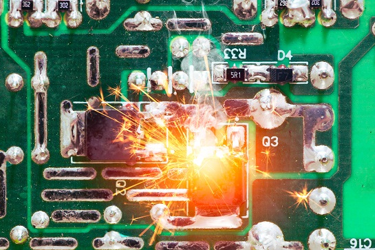
- Overheating: If there is no efficient thermal management, it can stress out a section of the board and cause it to burn out.
- Physical damage: This can be due to rough handling/dropping which results in cracks in components, solder joints, solder masks, traces, and pads.

- Contamination: If your board is exposed to harsh conditions, the traces and other copper features can be corroded.
How do you troubleshoot a PCB?
Troubleshooting techniques vary depending on the complexity of the design, including the number of layers, size, and density of components. Advanced boards may require special methods and equipment.
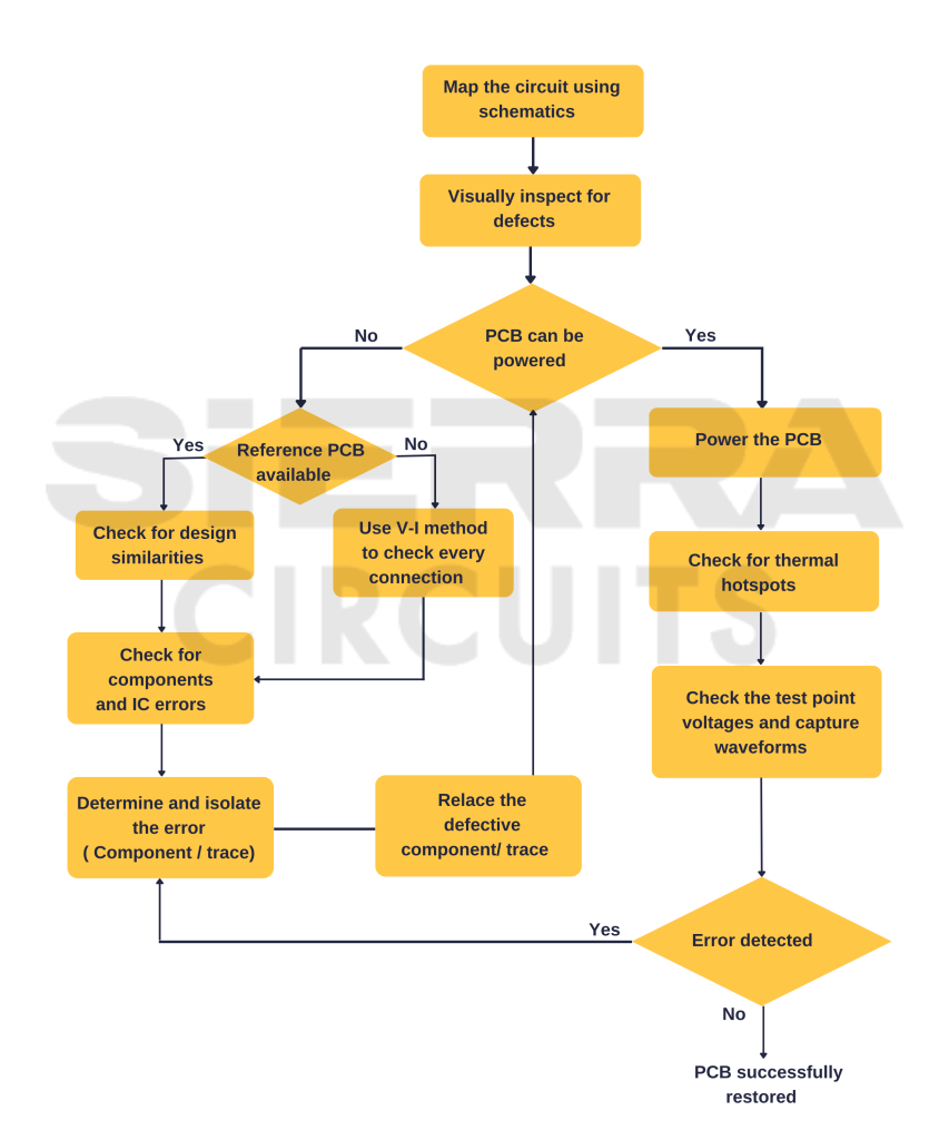
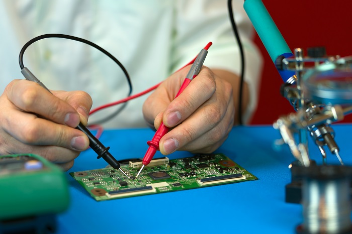
Tools required for inspection: For a simple circuit configuration, you can successfully troubleshoot a PCB only with a multimeter and test probes. But you may require an LCR meter, an oscilloscope, an external power supply, and a logic analyzer when handling more sophisticated designs.
1. Map out the circuit board
Generally, multiple components are connected through copper traces that extend to multiple layers on a circuit board. The board also has many sections like power supply, ground connections, and different signal attributes. It is also essential to know the location of filters, voltage dividers, decoupling capacitors, and chokes for an efficient PCB repair process.
All these require a good understanding of the schematics. Compare the circuit connections to the schematics and follow the current path to isolate the defective section. If you do not have access to the diagram, then you need to map it out manually by segregating every section. Analyzing the BOM may also be helpful.
2. Visually inspect surface elements
As mentioned above, excessive heat generation is one of the major issues for circuit board failure. If any of the components, traces, or solder joints are burned out, it is easy to detect visually with no input power. Other indicators of errors include:
- Bulging/overlapping/missing components
- Dulled traces
- Cold joints
- Excessive solder
- Tombstoning in solder joints
- Lifted/missing pads
- Cracks on the board
If defects are not visible to the naked eye, a magnifying glass or a microscope can help you examine them thoroughly.
3. Compare with an identical circuit board
If you have access to identical and operating circuit boards, it will be easier to troubleshoot the defective PCB. You can visually compare the misplacement and defects in components, traces, or vias. Additionally, check the input and output readings of both boards using a multimeter. It should read similar values, as both circuits have the same functionality and behavior.
4. Isolate defective components
When your senses can’t help, you need to use tools like a multi-meter and an LCR meter. Individually, test each component, such as resistors, capacitors, inductors, diodes, transistors, and LEDs, according to the datasheet and design requirements.
For example, you can inspect the diodes and transistors with the diode settings in the multimeter. The base-collector and base-emitter junctions act as diodes. If it’s a simple board design, you can check all the connections for open and short circuits. Just set the meter to ohms or the buzzer setting and start inspecting every connection.
While checking, if the reading is less than the specification, then the component is operating correctly. When the value is higher, there can be issues with parts or soldering joints. Knowing the expected voltages at testing points can help in analyzing the circuit.
Another way to evaluate the components is through nodal analysis. Here, you will not apply power to the whole circuit. Instead, the voltage is applied only to the selected component, and the voltage-to-current (V/I) response is measured. Next, identify all the nodes and choose a reference that connects important components or voltage sources. Calculate all the unknown node voltages (variables) using Kirchhoff’s current law (KCL) and verify if the values match. If you observe any discrepancies for a particular node, it means the node is faulty.
5. Test integrated circuits
This can be a difficult job, as ICs are inherently complex devices.
- Identify all the markings and use logic analyzers or oscilloscopes to test the IC.
- Check if the IC orientation is correct.
- Verify that all solder joints that connect to it are in good working order.
- Evaluate the conditions of the heatsink and thermal pads connected to the IC for good heat dissipation.
- If a similar operating IC is available, use it to evaluate the functional behavior of the circuit. This is one of the easiest ways.
6. Check the power supply
To troubleshoot the power supply, first, measure the rail voltages. The multimeter readings should reflect the input and output values expected at the component. There may be some problems in the circuit when there is a variation in voltage. For example, when the readings display 0 volts, there is a possibility of a short circuit along the power rail. This will result in overheating of the components. If you have conducted a power integrity test, you can compare the expected power values with the actual values to isolate the issue.
7. Determine the circuit’s hotspot
When you can’t find any visual defects, evaluate the circuit through physical inspection by injecting power. Faulty connections usually leave a hot spot, which can be felt by placing the hand over the board. You can also use a thermal camera. This test is usually preferred for low-voltage circuits. Necessary safety precautions should be taken to avoid electrical accidents. One of the methods is to ensure that you use only one hand for inspection. If you detect a hotspot, cool it and then search all the attached connections to identify the issue.
8. Troubleshoot using signal probing technique
To implement this technique, you must know the expected values and waveforms at all the test points. You can use a multimeter and an oscilloscope (or any wave-capturing device) to conduct voltage tests at different points. Analyze the results to isolate the errors. For instance, a lower voltage can be interpreted as leakage in the IC. The waveform will provide even more insights into the issue.
Tools required to repair a circuit board
Even before starting the board repair, ensure all essential tools are available.
- A table or workstation should have ESD grounding, power outlets, and proper lighting.
- Preheating the board may become necessary to limit the thermal shocks. Hence, keep an infrared heater or hotplate-type preheater.
- For making slots and holes during the repair process, you may need a good precision drilling system that lets you control the diameter and depth of the groove.
- Have a good soldering iron to create a proper solder joint while assembling the component. Use small tips to avoid excess flow.
- Apart from the replacement part, you need to have a variety of pads that will help in the mounting process.
- Next, in the repair process will be the plating. Ensure that you have an efficient system for achieving good plating without any harsh chemicals.
- It is better to use a two-part epoxy layer to restore the solder mask on the circuit, as it provides higher thermal resistance and mechanical stability. This will not be possible with one-part epoxy, even though it may set quickly. You may require a drying oven for the curing process.
Safety precautions during the PCB repair
It is better to take preventive measures to avoid accidents.
- Protective gear: When handling high heat or high power, it is essential to wear protective gear. Wear eyeglasses, gloves, and a mask during the soldering, drilling, or cutting process to avoid debris or chemicals.
- Electrostatic discharge: To prevent shocks due to ESD, ensure that you have unplugged and fully discharged the device. As mentioned, you can ground your workstation, wear grounded wrist straps, or use ESD-safe mats.
- Discharge the components: We all know that capacitors and a few other power supply components can hold a charge. Completely discharge all capacitors and batteries to avoid electric shocks.
How to repair printed circuit boards?
Normally, defects in traces, components, and pads are the causes of a circuit board failure.
Repairing broken traces
For repairing the broken/dulled trace, you need to expose the surface area of the original trace using a sharp object to remove the solder mask. This will help you get better electrical continuity. Clean the copper surface with a solvent to remove the debris. Solder a jumper or a wire to repair the trace. Ensure that the wire thickness is the same as the trace width.
To validate the trace width and spacing in your design, use the Better DFM tool.

Replacing defective components
While soldering, you apply heat and combine two metals using soldering iron, flux, and solder. Hence, to remove the solder joints of a defective component or excessive solder, you need to melt them. Remember to avoid creating thermal stress on nearby surface areas during the process. Follow these steps to replace the components in your board:
- Quickly heat only the required solder joint using a solder wick or desoldering station.
- When the solder joint melts, remove the liquid using a desoldering pump.
- Once you have removed all the joints, the component will detach.
- Next, assemble the new part and solder it.
- Cut off the excess length of the legs with the cutting pliers.
- Ensure the terminals are connected as per the required polarities.
Concealing the breaks in EMI or RF shielding
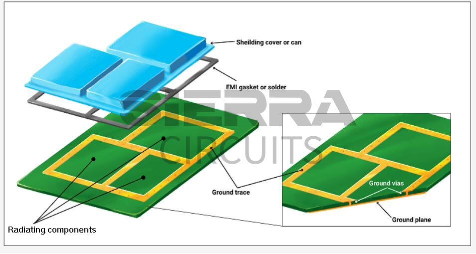
If mesh and metal screens are provided for EMI shielding, you need to ensure that their holes are smaller than the wavelength of the radiation. Hence, the meshes are designed with a conductive material and a constant pattern. If they are damaged or have cracks, use polyimide tape and conductive paint to restore them.
Restoring damaged pads
The pads on a circuit board can lift, corrode, or break over time. Here are the methods for salvaging the damaged pads:
Lifted pads: Clean them with a solvent using a swab. For adhesion, smear conductive epoxy onto the pad and press it down. Let the epoxy cure and proceed with the soldering process.
Broken or contaminated pads: Remove or cut the damaged pad. Scrape the solder mask around the pad to expose the connected trace. As usual, clean the area with a solvent using a swab. On the new pad (connected to the trace), apply a conductive epoxy layer and hold it in place. Next, add epoxy between the line and the pad. Cure it before the soldering process.
These are some of the important PCB troubleshooting and repair techniques. It is important to consider the complexity of the circuit, equipment availability, and condition of the board before you begin the restoration process. Make certain that you do not cause any additional damage to the board during these processes. Please leave a comment if there are any other repair methods you would like us to explain.
To learn the prerequisites of an error-free and cost-effective design, refer to the Design for Manufacturing Handbook.

Design for Manufacturing Handbook
11 Chapters - 96 Pages - 90 Minute ReadWhat's Inside:
- Annular rings: avoid drill breakouts
- Vias: optimize your design
- Trace width and space: follow the best practices
- Solder mask and silkscreen: get the must-knows
Download Now
About Sushmitha V : Sushmitha V has a master's degree in power electronics and has over four years of experience in the PCB industry. Her areas of interest include circuit board manufacturing, assembly, IPC standards, and DFM/DFA practices.