


Contents
Advanced electronics in aerospace applications experience temperature fluctuations. A good aerospace PCB thermal management system isolates sections with different temperatures and maintains the desired thermal operating environment. Hence, precise thermal control is mandatory for the prolonged functionality of electronic components on the board.
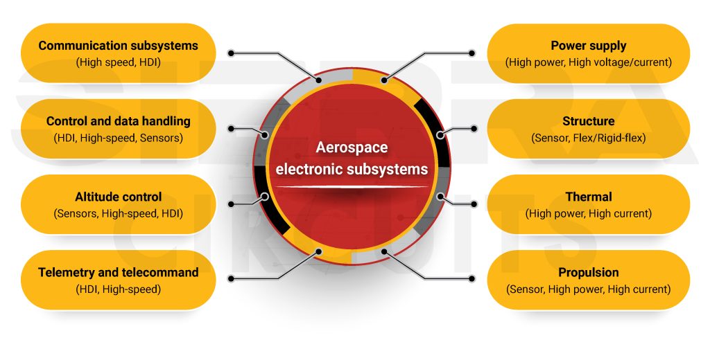
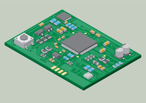
Aerospace subsystems use different categories of circuit boards, as shown in the image.
The graphic illustration below shows a few applications of PCBs in the aerospace industry:

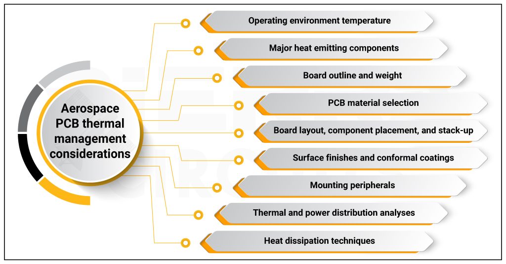
4 design guidelines for aerospace PCB thermal management
The typical operating temperature of an aerospace board is between –50 and 125ºC. Parameters that influence the thermal management system are discussed in this section.
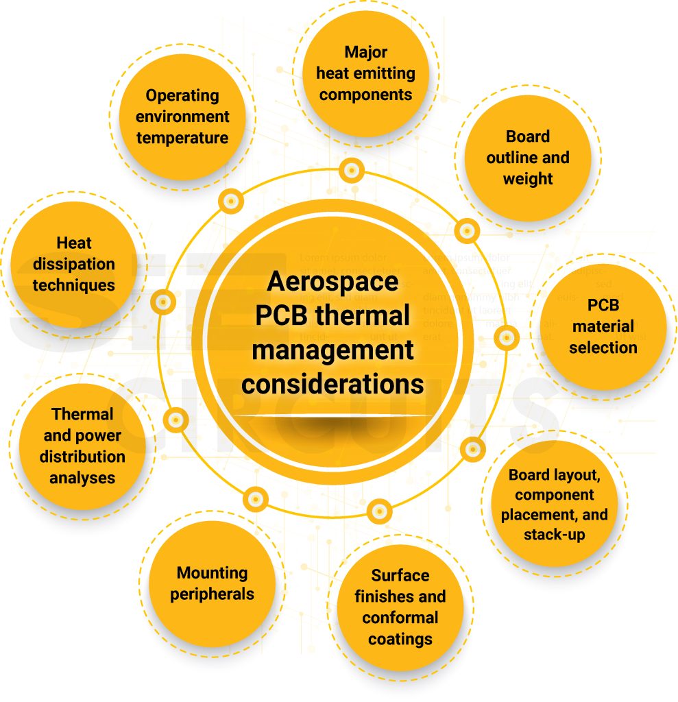
Selecting dielectric materials with excellent thermal properties, performing thermal analyses, and choosing the right heat dissipation strategies are some of the primary considerations when designing a thermal regulation system. Incorporating thick traces, thermal via stitching, and heat sinks are a few efficient circuit board thermal management techniques.
Focus on understanding how much heat is generated and how that heat is transferred around the circuit layout.
1. Choose a material with good thermal properties
Keep these benchmarks in mind while selecting materials for your aerospace designs:
- Low CTE (Z-axis expansion) (<70 ppm/ °C )
- High Tg (> 180 °C )
- High thermal conductivity (k)
- Low power losses at high speeds
- Dielectric constant (Dk) <4 (Typical value)
- High decomposition temperature (Td) > 360 °C
- Low moisture absorption
- Tight substrate weave
- Low outgassing rates
You can also opt for metal cores with high thermal conductivity. These cores will sink a lot of heat away from the components. Anodization of aluminum increases radiation heat transfer capability, corrosion and wear resistance, and surface emissivity. An example of the application of metal-core boards is LED lighting systems, as they generate a lot of heat. The metal core can act as a large ground plane in high-speed applications. They should be grounded to provide shielding and improve signal integrity.
Ceramic substrate materials have very high thermal conductivity and low electrical losses. However, they are brittle and can increase manufacturing costs. Aluminum oxide ceramics, like sapphire and alumina, are examples of such materials.
Polyimide is extensively used because of its good thermal capabilities. The recommended materials and their properties are shown in the table.
Choosing the right laminate is critical, but so is documenting its origin. To learn how materials are tracked throughout the board’s lifecycle, see what is traceability in PCB manufacturing?
| Material | Tg (°C) | Td (°C) | CTE Z-axis (ppm /°C) | Thermal conductivity (W/mK) |
|---|---|---|---|---|
| Isola FR408HR | 190 | 360 | 55 | 0.4 |
| Isola I speed | 180 | 360 | 60 | 0.4 |
| Isola P95 | 260 | 416 | 55 | 0.4 |
| Isola Astra | 200 | 360 | 50-70 | 0.45 |
| Panasonic Megtron6 R-5775 | 185 | 410 | 35 | 0.6 |
| Rogers RO4003 C | 280 | 425 | 46 | 0.26 |
| Rogers TTM10 | - | 425 | 20 | 0.76 |
| Rogers RO4350 B | 280 | 390 | 32 | 0.69 |
| Rogers RT/DUROID 5870 | - | 500 | 173 | 0.22 |
| Laird IMPCB | 165 | - | 36 | 2 |
| Nelco N7000-2HT | 260 | - | Improved <2.5% | 0.45 |
| Tachyon 100G | - | - | 45 (Pre-Tg) | 0.42 |

PCB Material Design Guide
9 Chapters - 30 Pages - 40 Minute ReadWhat's Inside:
- Basic properties of the dielectric material to be considered
- Signal loss in PCB substrates
- Copper foil selection
- Key considerations for choosing PCB materials
Download Now
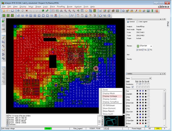
2. Perform thermal and power distribution analyses
These analyses provide a color-scale map of temperatures at various points on a PCB under different conditions. It identifies hotspots that help in:
- Understanding the heat flow pattern
- Checking dielectric material reliability with various CTE values
- Designing an efficient board layout, keeping component placement in mind. You will learn more about this in the next section.
- Component selection and heat sink design
- Selecting heat dissipation and cooling methods
- Avoiding device failures; improving product performance and durability
- Reducing project costs assures fewer engineering delays, field failures, and product iterations
Power distribution analysis can be carried out in some of the EDAs. There are many software applications available for thermal analysis, such as:
- Autodesk Fusion 360
- ANSYS
- Simscale
- 6 Sigma ET
- PICLS
- Adam Research
- Cadence Celsius Thermal Solver that can import files from Cadence Allegro
- Altium Designer allows easy export of design files to 3rd party PCB thermal simulation software
3. Select an appropriate surface finish like HASL
Surface finish and conformal coating act as a protective barrier against chemicals, corrosion, moisture, mechanical/electrical failures, and thermal stresses. The preferred surface finishes for reliable aerospace boards are gold, HASL, and ENIG. ENIG is the most economical and reliable for many applications as it has good polarity. It is inert, which reduces contamination reducing outgassing issues in your PCB.

Selecting a conformal coating material depends on the operating temperature range, condensation, repair, and tin whisker mitigation. Various coating materials are available, such as acrylic, urethane, silicone, epoxy, and parylene. They possess different properties suitable for various applications. Coatings with high thermal conductivity can help in better heat dissipation.
Parylene offers excellent penetration into cracks and is an ideal barrier and insulator. It has high thermal and UV stability. Therefore, it is a good choice for aerospace applications.
Christopher Young, President of Young Engineering Services, explained, ‘Immersion tin is a more suitable surface finish than gold plating, which can cause impedance mismatches.’ Here’s what Christopher Young, President of Young Engineering Services, says about aerospace PCB design challenges.
4. Adopt the right heat dissipation technique(s)
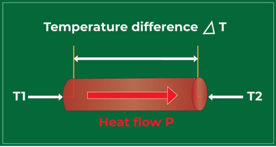
Thermal dissipation is a function of surface area, mass, and thermal resistance. Thermal resistance is the resistance to heat flow in a conductor.
Thermal resistance (R) ∝ Temperature difference (ΔT)/Heat flow (P) [K/W]
In this section, we discuss the heat dissipation strategies employed for aerospace PCB thermal management.
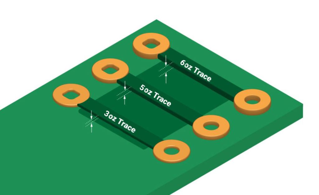
Employ heavy copper traces and ground planes for high-current designs
Increasing the thickness of traces and reference planes will increase heat dissipation through conduction and convection. The heavier the copper, the more heat can flow without restriction. Opt for thick copper traces (> 3 to 6 oz) for high-current designs to provide a low-impedance current path.
The thicker the copper trace, the wider the spacing between them to ensure manufacturability. This is called etch compensation. When elements are too close, it is difficult to etch down to the laminate before the copper features are reduced too significantly. They can even be etched away completely.
Using heavier ground planes (2 to 6 oz), you can dissipate heat. For better results, ask your manufacturer to mill its edges and slot them into the chassis.
Design cushioning: Adding extra design cushion or higher safety factors is a good practice to ensure that the applications will survive in extreme conditions. The extra cushion enhances durability and efficiency. For instance, a trace carrying a 1 amp current could be designed to carry 2 amps, which is a safety factor of 2 to prevent it from overheating.

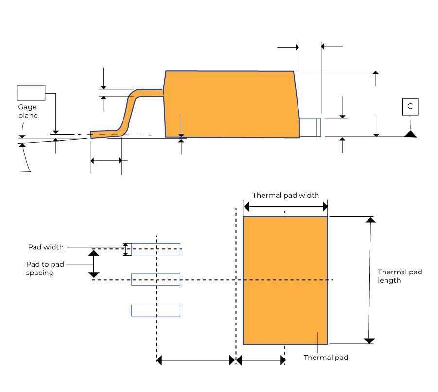
Place thermal copper pads under heat-emitting components
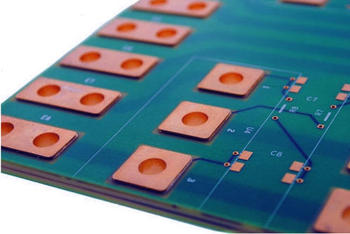
It is a large area of metal where you can solder devices or mount heat sinks for heat transfer. Some ICs have a thermal pad that can be connected to the ground plane through the substrate using thermal vias. When heat is transferred from a small landing pad to a pad with a larger area, it helps to cool down the heat source much faster. These heat spreaders can be rectangular or circular in shape. To ensure the desired soldering temperature and strong joints, carry out thermal profiling for heavy copper PCBAs.
Incorporate thermal vias to ensure a low resistance path from the top to the bottom layer
Thermal vias are through-hole contacts with enhanced copper plating thickness. These vias are placed below heat-prone components to vent out the heat. Also, too many vias can reduce the mechanical strength of your board, so choose the numbers and patterns wisely. Limitations of thermal vias are that they need a copper plane for dissipation, and their impact is limited to a localized area.
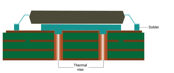
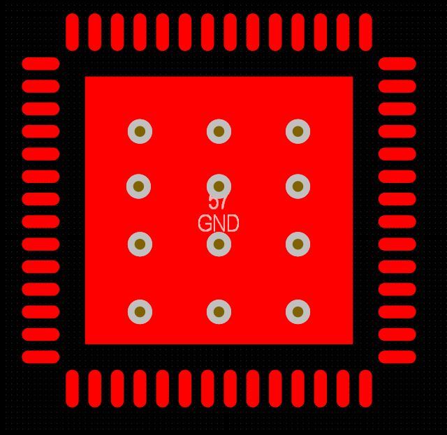
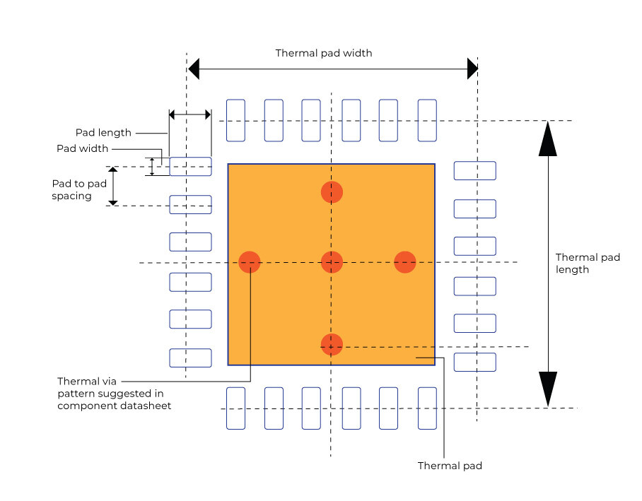
If the bottom conductor of the heated component is grounded, parallelly arranged vias are stitched to the ground plane, resulting in the lowest inductance return path. Vias can also be stitched to the heat sink for effective heat regulation. The number of thermal vias under power ICs is determined by considering the heat dissipation range, the pad’s surface area, via resistance, and their spacing.
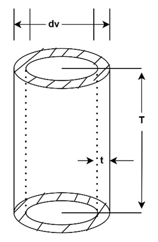
The thermal resistance of a via depends on its height, drill diameter, and plating thickness. The equation below can be used to calculate a via’s resistance.
![]() where,
where,
- dv is the drill diameter of the via hole
- t is the plating thickness
- dv-2t= Inner diameter of the plated hole and
- T= height of the via
Try our new Via Thermal Resistance Calculator. It determines the thermal resistance of vias by optimizing drill diameter and via-to-via spacing. This tool allows you to select two types of via patterns that suit your aerospace PCB thermal management. A list of commonly used conductive and non-conductive epoxy via fills and their thermal characteristics is also provided.
Implement heat sinks to transfer heat swiftly
A heat sink (HS) works on the principle of conduction, convection, and radiation. It transfers heat faster through convective airflow from the PCB to the fins, which provide a larger surface area. In your fab notes, mention that heat sinks should be attached using suitable thermal interface materials (heat sink compounds). Always ground the heatsink, as it can be a source of EMI.
Fins and spines are extended surfaces in heat sinks. Their design and performance are affected by the following factors:
- The thermal resistivity of the material used
- Heat transfer coefficient
- Thermal interface material used
- Number of fins and spacing between fins
- Mounting technique
Use this formula to calculate the heat sink junction-to-ambient thermal resistance:
Rja = Rjc + Rcs + Rsa
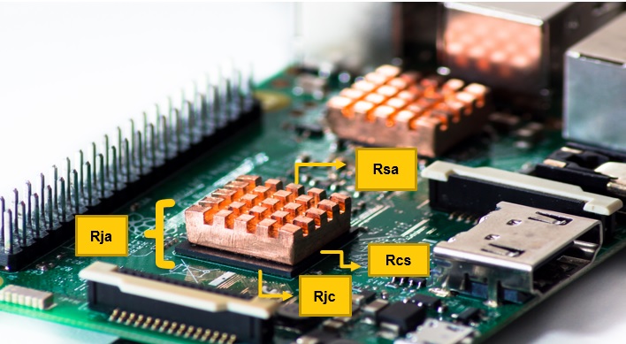
The maximum junction temperature can then be obtained using the equation below:
Tj = Ta + (Rja x Power dissipated)
where,
- Tj is the maximum junction temperature
- Rja is junction-to-ambient thermal resistance
- Rjc is junction-to-case thermal resistance
- Rcs is case-to-sink thermal resistance
- Rsa is sink-to-ambient thermal resistance
- Ta is the ambient temperature
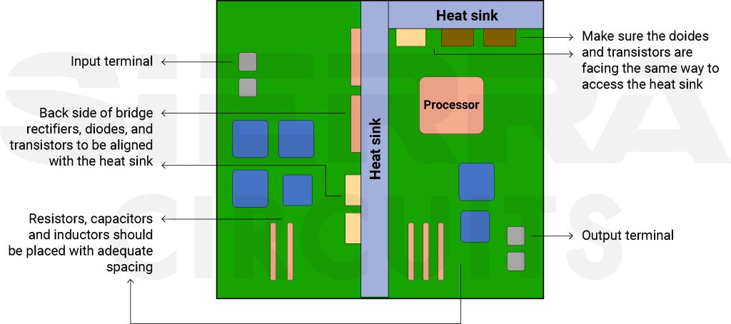
Fab notes for heat sinks
Always provide details with respect to heat sink placement and heat transfer requirements. This can be a separate document or part of your fabrication and assembly notes. Here’s an example assembly drawing.
Avoid solder wicking to reduce heat accumulation
To reduce heat accumulation on component leads, the soldering joint thickness should be even. Ask your manufacturer to take extra care while soldering near vias to avoid hole overfill with solder, as it reduces heat sink contact area.
Ways to avoid solder overflow are:
- Reduce the diameter of the via below 0.3mm. The smaller the vias, the better the surface tension of the liquid solder inside it. This helps in counteracting the force of gravity on the solder
- Implement solder mask tenting. It involves covering the pad of the via with a solder mask to prevent the solder from flowing down to the via.
For more on via tenting, see 6 common solder mask errors every PCB designer should know.
- Use via-in-pad-plated over where the via is filled with non-conductive epoxy to prevent solder from wicking into them

IPC Class 3 Design Guide
8 Chapters - 23 Pages - 35 Minute ReadWhat's Inside:
- IPC guidelines for manufacturing defects
- IPC standards for assembly processes
- Common differences between the classes
- IPC documents to set the level of acceptance criteria
Download Now
7 component placement guidelines for effective heat dissipation
- Use space-grade parts for utmost reliability with tight tolerances (1 to 2%) to accommodate the high current flow. Group components according to their thermal characteristics to incorporate effective localized heat dissipation strategies.
- Position sensors near the target area. Optimize design and construction based on their location in the spacecraft. For example, a thermistor should be placed at a point where the temperature needs to be controlled using a thermoelectric cooler (TEC).
- Evenly distribute active high-power components in your layout to prevent hotspots.
- Place heat-generating parts away from thermally sensitive devices to avoid component failure.
- Have µprocessors/µcontrollers at the PCB center so that heat scatters in all directions.
- Isolate low and high-frequency components for better signal integrity. For example, clock signals need to have proper physical shielding. It is also essential to reduce crosstalk.
- Ensure adequate spacing between high-power devices and adjacent copper features.
See component placement guidelines for PCB design and assembly to learn more about efficient part placement in your layout.
Types of thermal control systems used in aerospace applications
There are two types of aerospace thermal control systems (TCS): passive and active. Let’s discuss them in detail in this segment.
Passive thermal control systems
These systems maintain the constant temperature of components without using powered devices. A passive thermal management system works best in low-power and low-mass applications. They are mostly intended for lower heat loads with no moving parts.
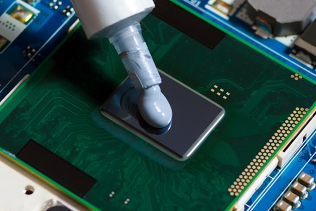
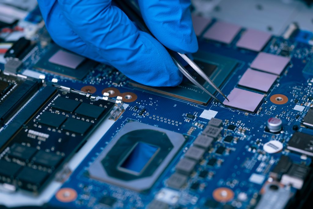
Thermal interface materials (TIMs)
These materials increase the conductive heat transfer between two components. These are advanced materials that quickly draw heat from active high-temperature components into a heat sink or enclosure wall. TIMs are available in various forms, such as grease, paste, gels, sheets, conductive adhesive tapes, or phase change materials. They can be employed between the mounting surface and heat-dissipating electronics to lower the temperature. For high heat-dissipating chips, thicker thermal gap pads are used on the PCBs. The choice of these materials depends on thermal conductivity, thickness, electrical isolation, temperature range, and life cycle.
Phase-change materials (PCM) can be waxes, paraffin, or salts that can change their phase by absorbing the heat. They are solid at room temperature and soften when heated. The gaps of contact surfaces are fully filled, resulting in a thin bond line without pump-out issues and increased reliability.
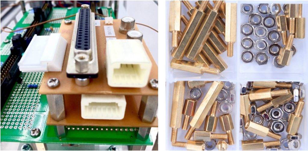
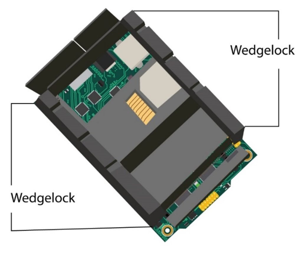
Mounting interfaces
Mounting interfaces facilitate the heat exchange between the PCB and structural elements. Heat dissipation can be increased using mechanical fasteners and washers to provide gaps between two or more PCBs.
Boards can also be mounted using wedge locks to transfer heat away from them to the enclosure, as shown in the figure.
Thermal straps
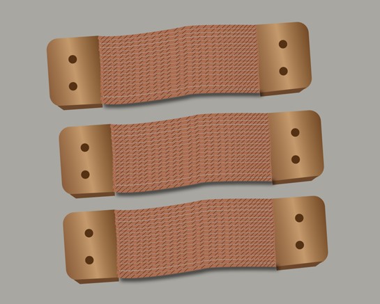
A thermal strap is a flexible link that transmits heat from a heat source to a sink. Often, these devices are utilized between high heat-generating chips/components and a chassis wall or radiator surface.
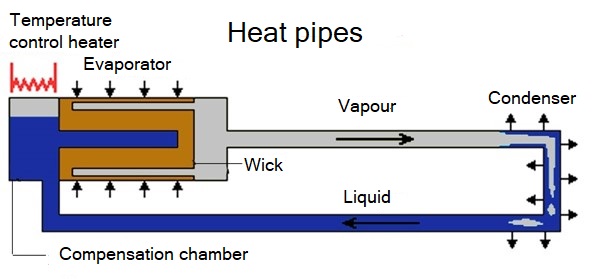
Heat pipes
They use a closed-loop system to carry the surplus heat through temperature gradients from electrical machines to a colder surface (radiator or heat sink).
Passive methods like multi-layer insulation (MLI), sun shields, and radiators are used to control the temperature of different aerospace sub-systems, including electronics. They either reduce heat loss from the aircraft or reduce heat radiation from entering the system.
Need help in designing reliable PCBs? Our engineering team can help you with thermal management, stack-up design, and DFM analysis.
You can book a meeting with our experts or call us at +1 (800) 763-7503.

Active thermal control system
Active TCS requires input power for operation, and it is more effective in controlling the stringent temperature needs of components. Aerospace PCB thermal management is carried out using cryocoolers, heaters, cold plates, and thermoelectric coolers. They have a quick response time and have moving parts.
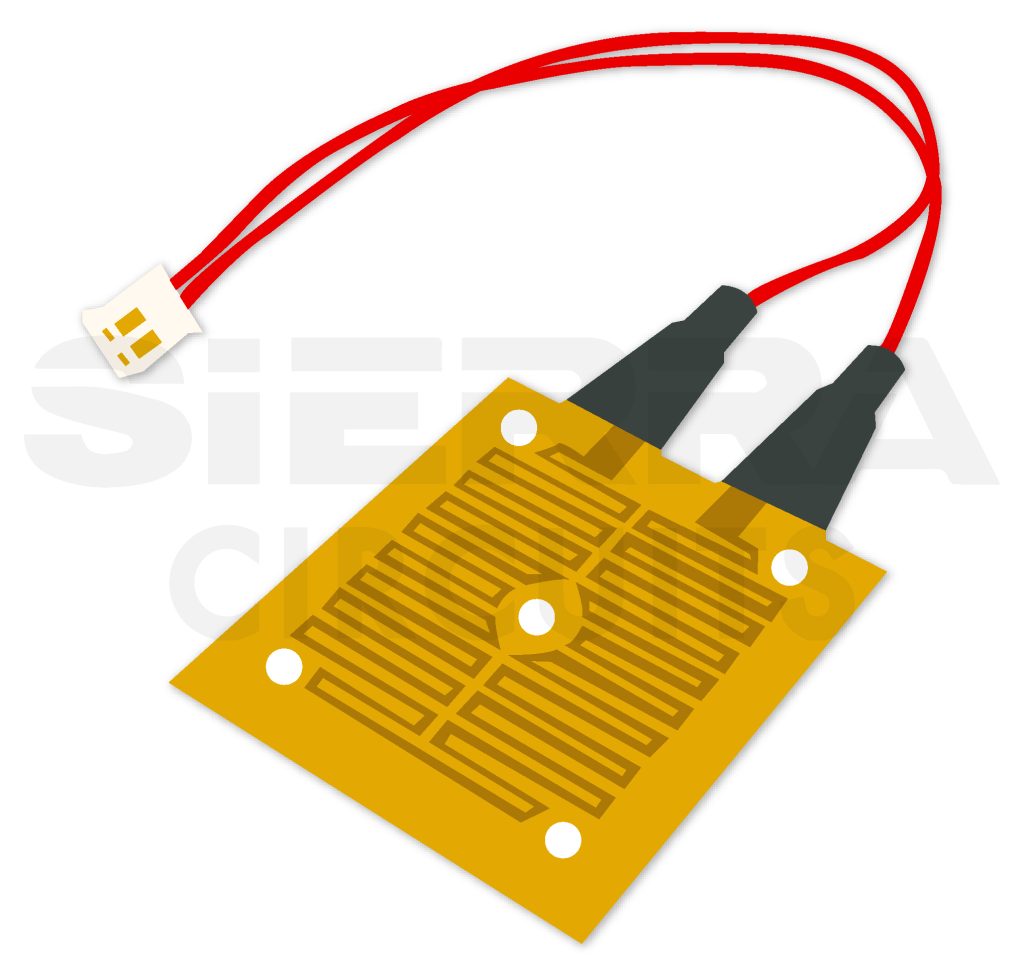
Heaters
Generally, small satellites require a low-power heater for temperature control. Small spacecraft employ Kapton heaters that include polyamide circuit boards. These heaters maintain battery temperature in cold environments. These devices control thermal regulations in eclipse and attain thermal stability.
Cryocoolers
Cryocoolers are used for maintaining extremely low-temperature environments (below 100K). These coolers are used for the low-temperature operation of high-precision IR sensors, interferometers, and spectrometers.
Cold plates
Cold plates are metal blocks (Al or Cu) that have inlets and outlets with internal tubing/mini-channels to allow liquid coolant to flow through to provide localized cooling. They transfer heat from the device to the ambient through a heat exchanger or to another liquid in a secondary cooling system. Liquid cooling provides efficient heat transfer compared to air cooling. The commonly used fluids are water, inhibited glycol and water solutions, dielectric fluids, or nanofluids. Cold plates are an essential part of closed-loop liquid cooling.
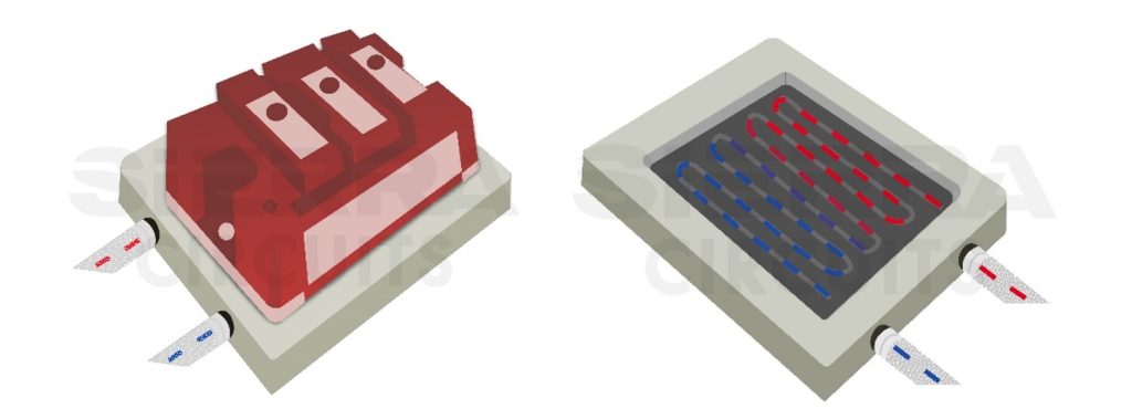
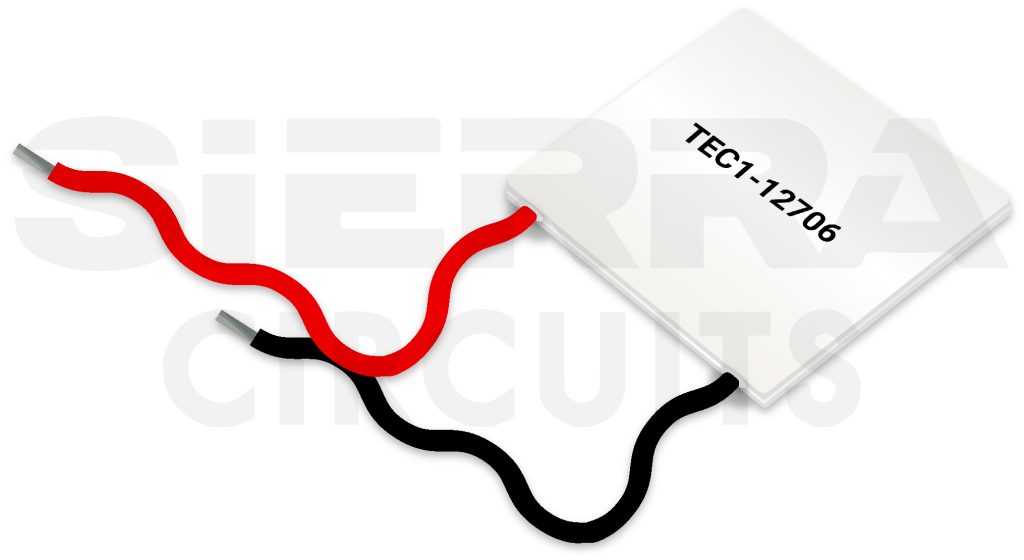
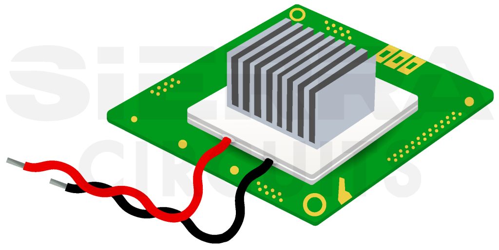
Thermoelectric cooler (TEC)
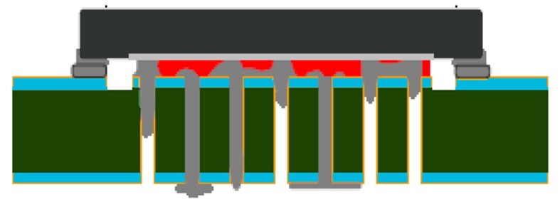
TEC systems cool components to sub-ambient temperatures and offer accurate temperature control and faster response. They are used in CCD cameras (charge-coupled devices), laser diodes, microprocessors, and night-vision systems. TEC uses the Peltier effect to transfer heat using a heat exchanger. The principle of the Peltier effect is that the electric current flowing through a junction will emit or absorb heat to stabilize chemical potential differences.
The images below illustrate a thermo-electric cooler and its mounting.
For more aerospace PCB design tips, see 14 aviation and aerospace PCB design rules for high-reliability
Aerospace PCB thermal management is of critical importance for the proper functioning of electronic subsystems in space vehicles. You can effectively regulate the heat generated in these boards by selecting materials with good thermal properties and choosing space-grade components.
The placement of parts should ensure even heat distribution on your board. Use heat dissipation techniques like heavy copper traces and layers, thermal via stitching, heat sinks, thermal copper pads, and TIMs in your design. Understand the AS9100 standard and IPC class 3 specifications for space/military applications to build a reliable circuit board.
See aerospace and defense PCB standards designers should know, to learn about the standards that apply to aviation and space applications.
We interviewed Paul Cooke on PCBA aerospace thermal control systems. Paul Cooke, Field Application Manager at AGC to speaks about thermal interfaces, reliability, and heat dissipation in aerospace boards.
Visit Sierra Circuits’ certifications and registrations page to learn about the standards to which we conform.
Have queries on PCB thermal management? Post them on our forum, SierraConnect, and our experts will resolve them.


Start the discussion at sierraconnect.protoexpress.com